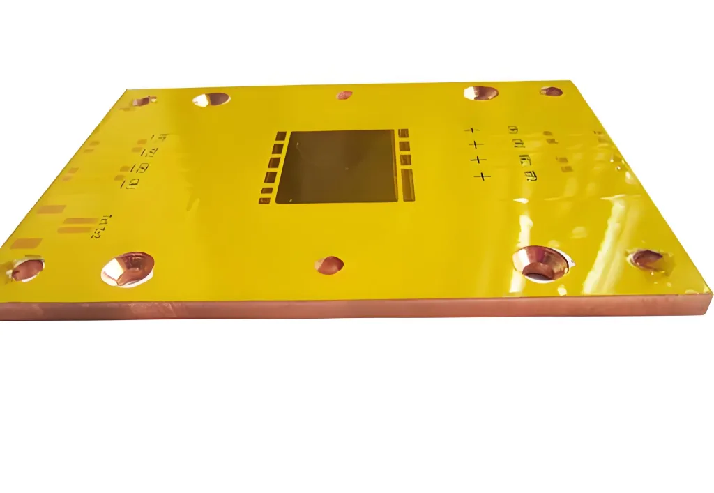
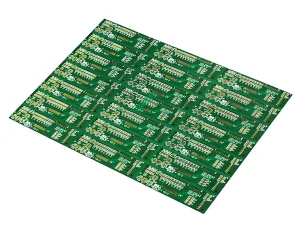
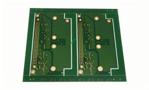
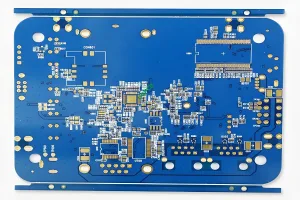
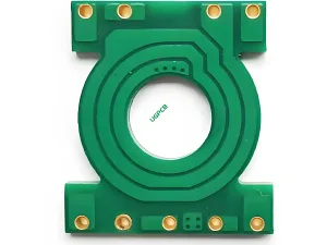
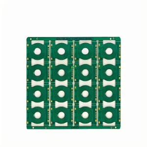
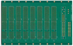
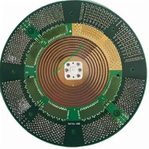
4-Layer Gold-Plated Copper Substrate Product Overview
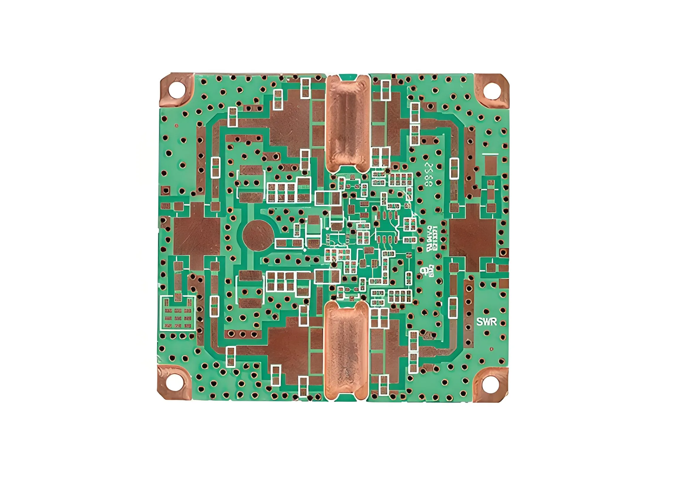
Gold-Plated Copper Substrate
The 4-layer gold-plated copper substrate is a type of high-performance, highly stable, and reliable high-frequency PCB board. It is suitable for high-end electronic products that require high thermal conductivity, high electrical conductivity, 高い信頼性, good machining performance, and signal transmission capabilities.
Advantages of the 4-Layer Gold-Plated Copper Substrate

Gold-Plated Copper Substrate
1. High Thermal Conductivity
The copper substrate has high thermal conductivity, allowing for rapid heat transfer and improving thermoelectric conversion efficiency.
2. High Electrical Conductivity
The copper substrate has high electrical conductivity, enabling quick electron transmission, enhancing the generation of the thermoelectric effect, and increasing current output.
3. Good Mechanical Properties
The copper substrate has high strength and hardness, along with good corrosion resistance, making it suitable for various application environments.
4. Excellent Machining Performance
The copper substrate is easy to cut and form, allowing it to be prepared into devices of various shapes and sizes, suitable for various application scenarios.
5. High Reliability
The copper substrate uses high-quality materials and manufacturing processes, providing high reliability and stability.
6. Gold Plating Treatment
The surface of the copper substrate undergoes gold plating treatment, offering better signal transmission performance and stability.
 UGPCBのロゴ

