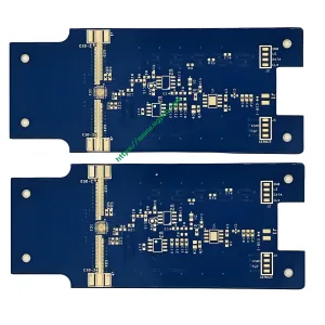
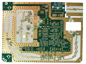
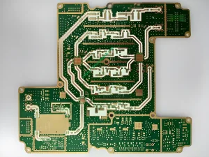
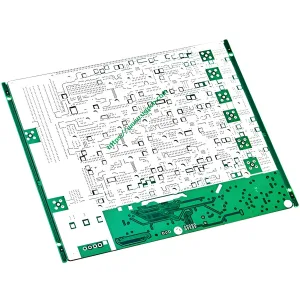
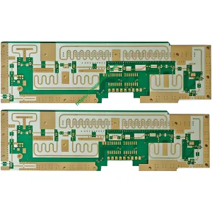
Overview of High Frequency PCB
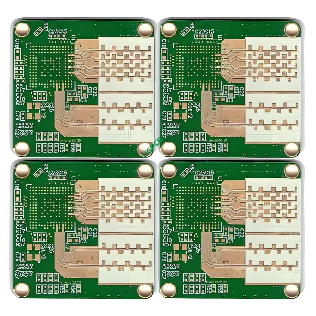
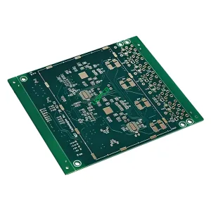
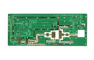
A high-frequency PCB is a specialized type of circuit board designed to operate at high frequencies, typically in the range of gigahertz (GHz). These PCBs are essential for applications that require precise signal transmission and minimal signal loss. They are widely used in industries such as telecommunications, レーダーシステム, and satellite communications. The quality standard for high-frequency PCBs is IPC 6012 クラス 2, ensuring high reliability and performance.
定義と重要な仕様
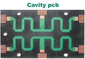
A high-frequency PCB is defined by its ability to handle signals at very high frequencies while maintaining signal integrity. 誘電率 (dk) of these PCBs ranges from 2.0 に 1.6, which is crucial for controlling signal speed and impedance. The number of layers can vary from 1 に 36, providing flexibility for different design requirements. The thickness of the PCB ranges from 0.254mm to 12mm, and the copper thickness can be either 0.5oz or 1oz. Surface technologies include Silver, 金, and OSP, each offering different benefits in terms of solderability and corrosion resistance. Special processes like mixed materials and stepped grooves further enhance the performance of high-frequency PCBs.
設計上の考慮事項
When designing a high-frequency PCB, いくつかの要因を考慮する必要があります:
- 誘電率 (dk): The dk value between 2.0 そして 1.6 is critical for maintaining signal integrity at high frequencies.
- レイヤー数: The wide range of layer options (1 に 36) allows for customization based on specific application needs.
- 厚さ: The thickness range from 0.254mm to 12mm provides flexibility in design, catering to different spatial and functional requirements.
- 銅の厚さ: The choice between 0.5oz and 1oz base copper affects the current-carrying capacity and signal integrity.
- Surface Technology: Options like Silver, 金, and OSP provide different levels of solderability and corrosion resistance.
- 特別なプロセス: Techniques like mixed materials and stepped grooves can significantly enhance the performance of high-frequency PCBs.
作業原則
High-frequency PCBs operate based on the principle of controlled impedance and minimal signal loss. The dielectric constant of the materials used ensures that signals travel with minimal delay and loss, 彼らの完全性を維持します. 厚さと銅の重量を正確に制御すると、一貫したインピーダンスが可能になります, これは、高周波信号伝送にとって重要です. Surface technologies like Silver, 金, and OSP provide reliable connection points for components, 効率的な信号伝達を確保します.
アプリケーション
High-frequency PCBs are used in a variety of applications that require high-speed data transmission and signal integrity:
- Telecommunications: Ensuring clear and reliable signal transmission in mobile phones, base stations, and other communication devices.
- Radar Systems: Providing accurate and reliable signal processing in military and civilian radar systems.
- Satellite Communications: Facilitating rapid and reliable data transfer between ground stations and satellites.
分類
High-frequency PCBs can be classified based on several criteria:
- Frequency Range: Typically operating at gigahertz (GHz) frequencies.
- レイヤー数: 範囲から 1 に 36 レイヤー, 回路の複雑さに応じて.
- 厚さ: Options from 0.254mm to 12mm allow for customization based on specific application needs.
- 銅の厚さ: Standard and heavy copper options (0.5oz and 1oz) cater to different current-carrying capacities.
- Surface Technology: Choices like Silver, 金, and OSP provide different levels of solderability and corrosion resistance.
材料特性
The key properties of high-frequency PCB materials include:
- 低誘電率: 信号の遅延と損失が最小限に抑えられます, making them suitable for high-frequency applications.
- 広い厚さの範囲: 設計の柔軟性を可能にします, catering to different spatial and functional requirements.
- Excellent Signal Integrity: 高周波数でも信号の完全性を維持します, 信頼できるパフォーマンスを確保します.
- Reliable Connection Points: Surface technologies like Silver, 金, and OSP provide strong and reliable connection points for components.
製造工程
The production of a high-frequency PCB involves several steps:
- 材料の選択: Choosing materials with a low dielectric constant and high signal fidelity.
- 回路設計: 高周波性能と信号の完全性に関する考慮事項を備えた回路レイアウトの作成.
- エッチング: 不要な銅を除去して、目的の回路パターンを作成します.
- ラミネート加工: 強力で信頼できる接続を確保するために、高圧と温度の下で複数の層を結合する.
- 表面仕上げ: Applying surface technologies like Silver, 金, or OSP to enhance solderability and corrosion resistance.
- 特別なプロセス: Utilizing techniques like mixed materials and stepped grooves to further enhance performance.
- テストと品質管理: 最終製品がすべての仕様と標準を満たすようにします.
シナリオを使用します
High-frequency PCBs are used in scenarios where high-speed data transmission and signal integrity are critical:
- Mobile Phones: Ensuring clear and reliable signal transmission in modern smartphones.
- Base Stations: Providing accurate and reliable signal processing in communication infrastructure.
- Radar Systems: Enabling precise and reliable signal processing in military and civilian radar applications.
- Satellite Communications: Facilitating rapid and reliable data transfer between ground stations and satellites.
要約すれば, high-frequency PCBs are specialized circuit boards designed for high-speed data transmission and signal integrity. Their low dielectric constant, 広い厚さの範囲, and excellent signal fidelity make them ideal for applications in telecommunications, レーダーシステム, and satellite communications.
 UGPCBのロゴ

