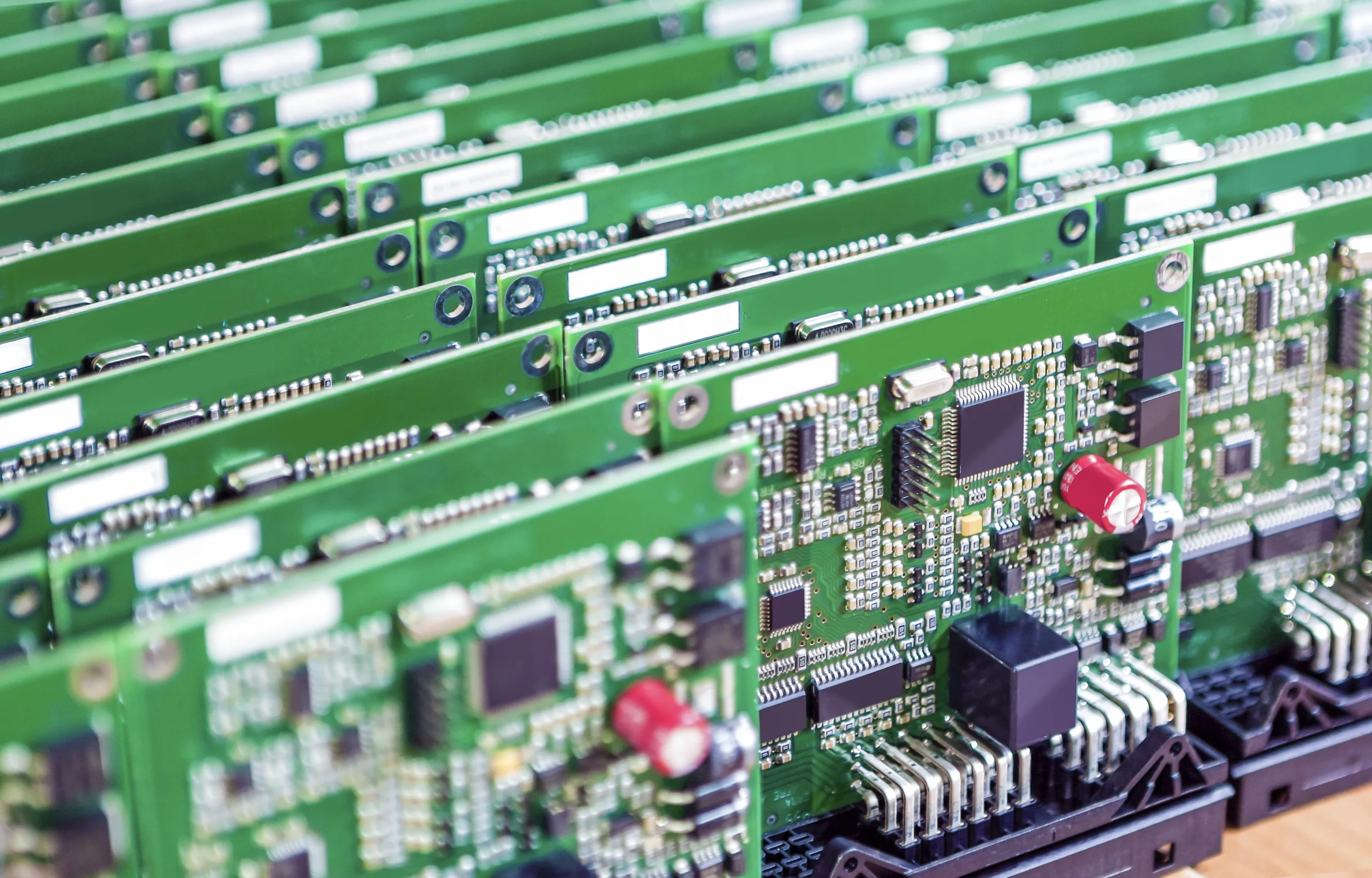
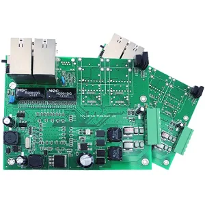
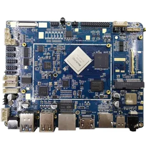
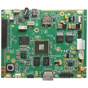
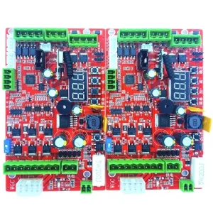
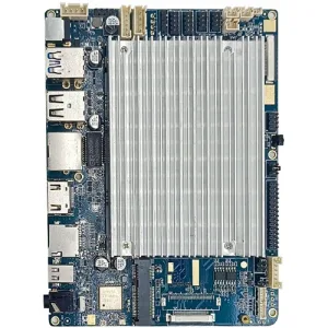
The cleanliness of electronic PCB components can enhance the reliability of medical devices.
Overcoming the possibility of failure.
Component manufacturers are constantly developing new and smaller packages for components, which are only a fraction of a millimeter in size, and the gap between the board and the component is less than one mil. The pick-and-place machines have new attachments that can place these almost invisible parts. Components are placed very close together. How do you effectively clean something so small?
Lead-free solder is a relatively new legislative fact, requiring new solders, new fluxes, higher temperatures, and new soldering equipment. Many new methods, alloys, 化学物質, and soldering processes have been developed to address these issues. The problem of tin whiskers has also increased sharply. しかし, delayed effects usually do not show up until one or two years after the product leaves the factory and is put into use. The speed of product development masks some of these time-delayed issues because products are often discarded for newer models. Products like mobile phones generally do not experience problems because there are few people who use a phone for more than 2-3 年. Few people will spend money on repairs when feature-rich upgrade models are offered at subsidized prices. しかし, for medical devices, the possibility of failure is very high, and the impact of failure could be devastating.
Design decisions affect other process steps.
All of this comes together and where support elements must function properly is in the manufacturing workshop, but component manufacturers, circuit board designers, and equipment manufacturers often operate independently of each other. This communication gap exacerbates the problem. Research shows that many failures are due to insufficient cleaning of contaminants during the printed circuit board (プリント基板) manufacturing process. Advanced CAD design systems used for PCB design can cause some design issues.
時々, designers utilize features such as ultra-close copper cladding or filled copper, bringing the entire circuit board’s grounding distance from the power bus by just a few mils. The chances of catastrophic shorts increase several times over. Many designers rarely encounter production issues with PCB manufacturing or circuit board assembly. For circuit board designers, it is crucial to understand how flux flows next to connector pads during manual soldering of connectors. Many decisions made during implementation affect other process steps.
Higher standards needed for high reliability.
IPC serves as a global trade association for the printed circuit board and electronic assembly industry, its customers, and suppliers. Its working groups are dedicated to addressing all topics related to determining the cleanliness levels of unassembled (bare) printed circuit boards and have established basic standards for cleaning. The IPC-TM-650 standard sets an acceptable range of 10-2 micrograms/in² sodium chloride (NaCl) for military applications (general applications are 65-2 micrograms/in²). Is this standard sufficient to prevent failures, and can current cleaning methods truly clean today’s produced circuit boards?
Many myths circulate in the industry:
- All bare boards from the factory are clean.
- All components are delivered clean without contamination issues.
- Flux will not cause any problems; just pour it on the board, no need to worry about heating or not heating, everything will be fine.
This is not the reality of today’s manufacturing, but the assumptions behind these concepts pose significant problems for manufacturers. Circuit boards with hidden residual flux contamination may pass QC and work normally. Once they reach their working environment, high humidity and temperature fluctuations can occur, leading to condensation and causing residual flux problems to really start growing, eventually leading to leakage paths and ultimately failure. Today’s micropower electronic equipment’s high impedance circuits are more easily disturbed by stray voltage sources.
Simple washing is not enough.
Cleaning printed circuit boards after the soldering process often results in shiny boards that seem ready for the next journey of the end user. Invisible areas contain details that destroy this shiny clean picture. Simply putting the circuit board through a cleaning cycle is not enough. It requires a special combination of chemicals, 温度, cleaning cycles, and timing to truly clean the circuit board.
“The cleanliness of printed boards directly affects the efficiency or quality of assembled printed boards,” says John Perry, IPC Technical Program Manager and Staff Liaison for the IPC Task Group on Bare Board Cleanliness Assessment. “Residues increase the risk of field failures or can hinder the functionality of printed boards, therefore having acceptance criteria with different levels of testing and direction on how many samples should be tested is very important.”
Digital Tong Electronics has utilized extensive resources to study these issues. 多くの場合, we find that relatively small points combined indicate processes that simply cannot work in today’s manufacturing environment, even though they were sufficient in the past. Minor changes in component packaging design, 材料, CAD/CAM software, circuit board manufacturing, and chemistry combine to slowly change the robustness of the manufacturing process. Even the best intentions often unconsciously create possibilities for defects to occur in ways previously impossible. Only through a comprehensive assessment of all materials and steps in the manufacturing process can the root causes of potential problems be identified. With a clear understanding of potential problem areas, much effort is needed to find solutions to each problem.
New equipment and support subsystems were ordered and installed. Testing and evaluation procedures were developed and implemented to verify the effectiveness of each process. All circuit boards are regularly run through the system before and after the assembly process to ensure that the soldering process is not affected by any contaminants from the circuit board manufacturing process, and that the circuit board is completely free of any chemicals remaining from the soldering process.
The cleaning process is completely green. Deionized water from the polishing tank is used and recycled. Filters capture solids, while powerful blowers ensure that irritating chemicals do not migrate through the tank. Transparent windows on the equipment allow operators to monitor the entire process. A refractometer checks the stability of the mixture in the tank to ensure it is undamaged. The discharged liquid is completely environmentally friendly.
The process is then thoroughly tested, evaluated for effectiveness, and finally verified as a stable process. Independent tests show that circuit boards cleaned through this process are 75% cleaner than the highest level of cleanliness specified by IPC, それは 10-2 micrograms/in². さらに, laboratory analysis of ion contamination found zero sodium chloride ion contamination on the assembled boards.
UGPCB supports the business of medical PCB board blood pressure meter PCBA assembly supplier. We are a professional PCBA one-stop assembly factory, welcome to place orders!
 UGPCBのロゴ
