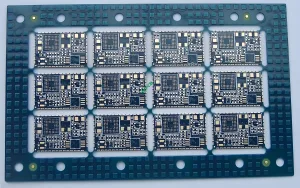
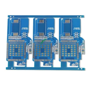
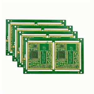
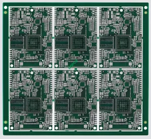
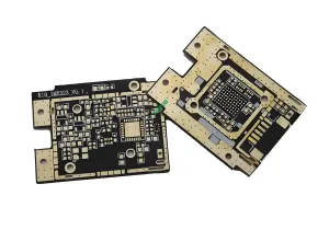
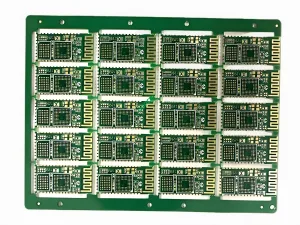
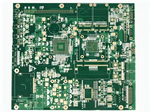
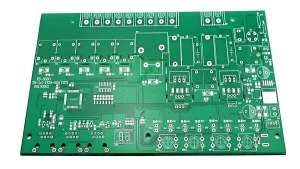
What is ENIG PCB?
同意する (Electroless Nickel Immersion Gold), also known as gold immersion (AU), electroless Ni/AU, or soft gold, is a metal plating process used in the manufacture of printed circuit boards (プリント基板) to prevent copper oxidation and improve touch and through-hole plating.
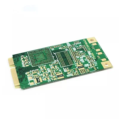
- 製品詳細
 UGPCBのロゴ

