Various Names of Circuit Boards
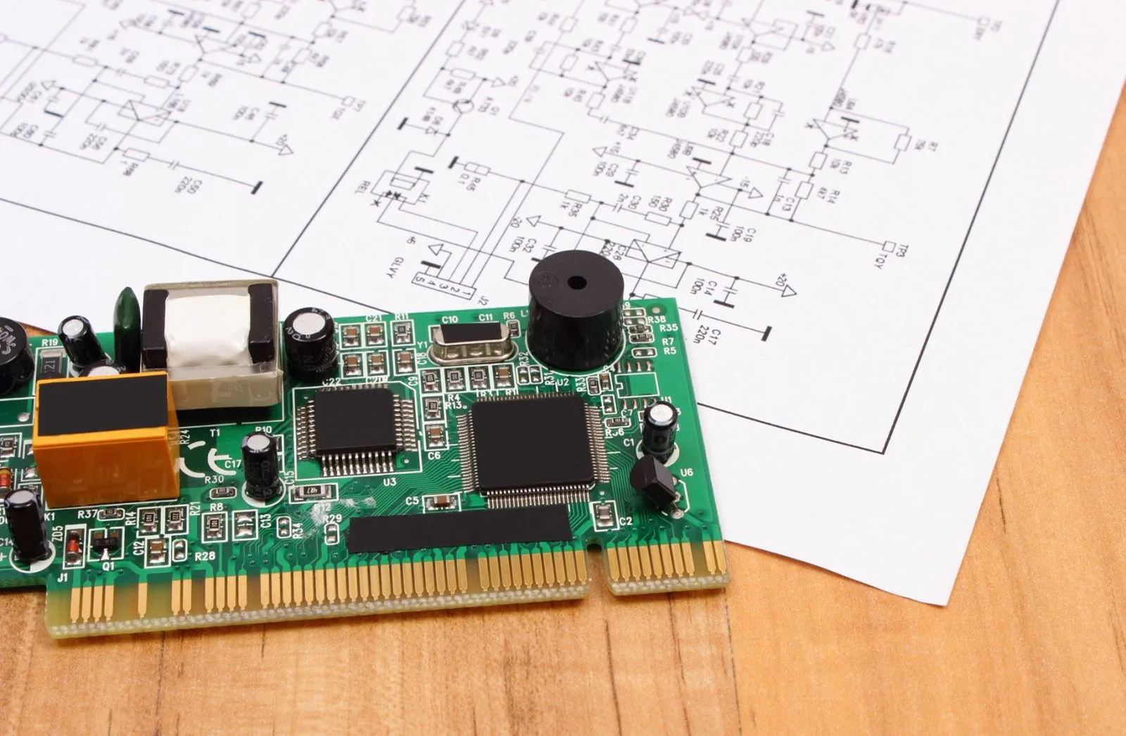
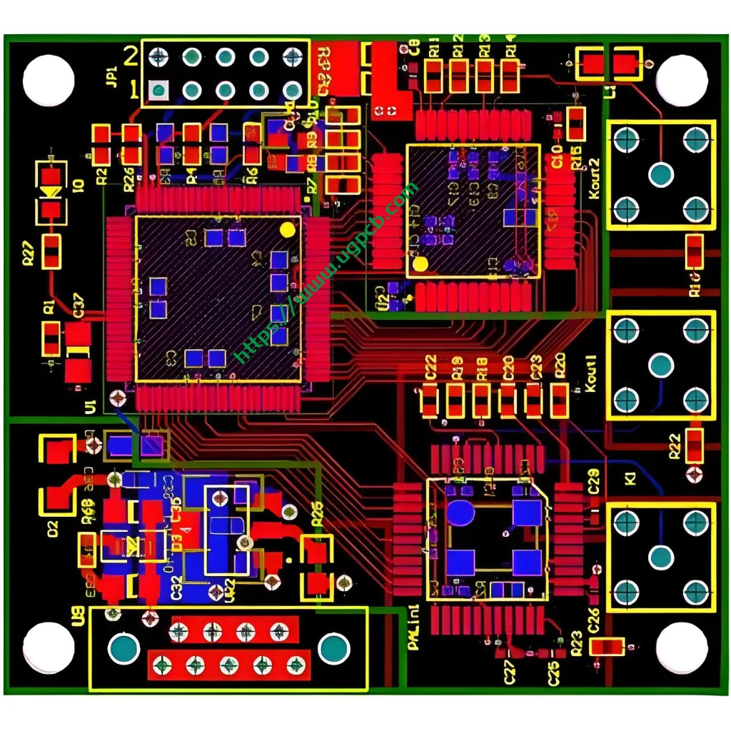
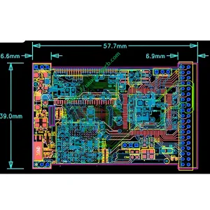
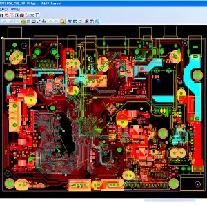
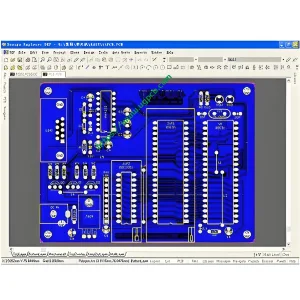
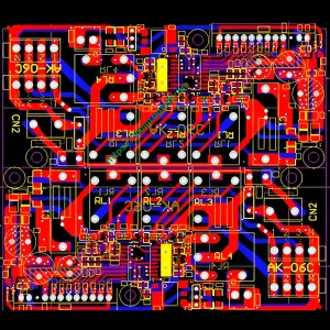
The names of circuit boards are: セラミック回路基板, alumina ceramic circuit board, aluminum nitride ceramic circuit board, 回路基板, PCBボード, aluminum substrate, high frequency board, thick copper board, impedance board, プリント基板, ultra-thin circuit board, Thin circuit boards, 印刷された (copper etching technology) circuit boards, 等.
Importance of Circuit Boards
The circuit board makes the circuit miniaturized and intuitive, and plays an important role in the mass production of fixed circuits and the optimization of the layout of electrical appliances.
Types of Circuit Boards
プリント基板 (プリント基板)
Circuit boards can be called printed circuit boards.
FPC Circuit Boards
FPC circuit boards (also known as flexible circuit boards) are a kind of high reliability made of polyimide or polyester film as the base material. They are an excellent flexible printed circuit board with the characteristics of high wiring density, 軽量, 薄い厚さ, and good bendability.
Soft-Rigid Board
The birth and development of the flexible and rigid combination board—FPC and PCB, gave birth to the combination of flexible and rigid board this new product. したがって, the soft-rigid board is a circuit board with FPC characteristics and PCB characteristics formed by combining flexible circuit boards and rigid circuit boards according to relevant process requirements through lamination and other processes.
 UGPCBのロゴ
