
Electroless Nickel Palladium Goldの概要
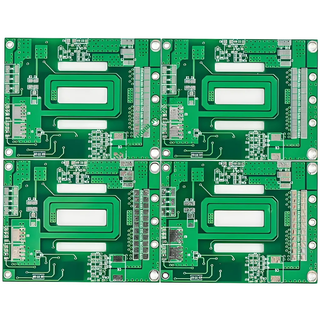
エレクトロレスニッケルパラジウムゴールドは、印刷回路基板産業における重要な表面処理プロセスです. ハードサーキットボードの生産プロセスで広く使用されています (プリント基板), 柔軟な回路基板 (FPC), 厳格なスクランブルボード, および金属基板. また、将来の印刷回路基板産業における表面処理の重要な開発動向です.
プロセスとメカニズム
エレクトロレスニッケルパラジウムゴールドは、ニッケルの層を堆積させる非選択的表面処理技術です, パラジウム, 化学的方法による印刷回路の銅層の表面上の金. 主なプロセスフローはです:
- 脱脂
- マイクロエッチング
- 事前に浸る
- Activation
- Nickel plating
- Palladium plating
- Gold plating
- Drying
There will be multi-stage washing treatment between each link. The mechanism of electroless nickel-palladium-gold reaction mainly includes redox reaction and displacement reaction. その中で, the reduction reaction is easier to deal with thick palladium and thick gold products.
現在のところ, the production specifications of chemical nickel, パラジウム, and gold in general factories are: nickel 2-5um, palladium 0.05-0.15um, and gold 0.05-0.15um. もちろん, due to differences in plant equipment and reaction mechanisms, the uniformity of chemical reactions and the ability to handle thick palladium and thick nickel are also different.
Comparison with Electroplating Nickel Gold
Application and Production Capacity
Electroless nickel palladium gold is also an important surface treatment process in the field of printed circuit boards. 主なアプリケーションフィールドは、ワイヤボンディングテクノロジーです, ハイエンドの電子回路製品にある程度対処できます.
化学ニッケルパラジウムゴールドの反応速度は遅いです, リードワイヤと電気めっき線の接続を必要としないため, 同じ量のタンクで同時に生産された製品の数は、電気めっきニッケルゴールドの製品よりもはるかに大きいです. したがって, 全体的な生産能力の優位性が非常に大きくなっています.
開発動向
前述のとおり, エレクトロレスニッケルパラジウムゴールドの主な利点は、ハイエンド製品と細かい回路の表面処理に対処することです. しかし, 電子技術の開発とそのアテンダントの要求も急速に成長しています. 現在のところ, 一般的な化学ニッケルパラジウムゴールドプロセスは、徐々に高精度回路の生産に対処できなくなります.
したがって, より高い需要に対処するため, 現在の主な開発の方向は、薄いニッケルパラジウムゴールドテクノロジーと化学パラジウムゴールドテクノロジーです. これらのテクノロジーは、通信に広く使用されています, 家電, 産業用制御, 安全, 自動車, 電源, スマートホーム, 医学, 軍隊, その他の産業.


