Overview of Panasonic M6 High Speed PCB
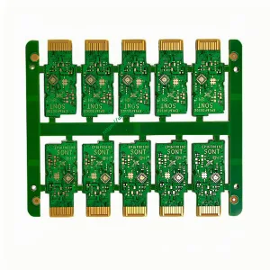
The Panasonic M6 high speed PCB is a cutting-edge product designed for high-performance applications, particularly in the field of optical modules. This 8-layer printed circuit board (プリント基板) boasts a finished thickness of 1.0mm and is made from high-quality materials to ensure optimal performance. With its green or white color options and electric hard gold surface treatment, this PCB is tailored for demanding electronic environments.
Definition and Design Requirements
A high-speed PCB is specifically engineered to handle high-frequency signals with minimal loss and interference. The design requirements for the Panasonic M6 include:
- Layer Configuration: 8 layers to support complex circuitry and signal routing.
- Material Quality: Utilizing Panasonic M6 material known for its superior dielectric properties.
- 厚さ: A standard finished thickness of 1.0mm ensures durability and stability.
- Copper Weight: Available in 0.5OZ and 1OZ to accommodate different current-carrying capacities.
- カラーオプション: Offered in green and white for easy visual identification during manufacturing.
Working Principle
The working principle of the Panasonic M6 high speed PCB revolves around its ability to manage high-speed data transmission efficiently. Key aspects include:
- Electric Hard Gold Surface Treatment: Enhances conductivity and prevents oxidation.
- Golden Finger Bevel Technology: Improves insertion and extraction reliability in connectors.
- 最小トレース/スペース: At 3mil/3mil, it supports fine line definition crucial for high-density interconnects.
アプリケーション
Primarily used in optical module applications, these high-speed PCBs are integral in devices requiring rapid data processing and transmission, such as telecommunications equipment, data centers, and high-speed networking gear.
Classification and Materials
This high-speed PCB can be classified based on its application needs, レイヤー数, and specific electrical characteristics. The primary material, Panasonic M6, is chosen for its excellent high-frequency performance, 低い誘電率, and minimal signal loss.
Panasonic M6 high speed PCB material general properties
| Item | Test method | 状態 | ユニット | メガトロン6 R-5775(N) Low Dk glass cloth |
メガトロン6 R-5775 Normal glass cloth |
|
| Glass transition temp.(TG) | DSC | あ | ℃ | 185 | 185 | |
| Thermal decomposition temp.(TD) | TGA | あ | ℃ | 410 | 410 | |
| CTE x-axis | α1 | IPC-TM-650 2.4.24 | あ | ppm/°C | 14-16 | 14-16 |
| CTE y-axis | 14-16 | 14-16 | ||||
| CTE z-axis | α1 | IPC-TM-650 2.4.24 | あ | 45 | 45 | |
| α2 | 260 | 260 | ||||
| T288(with copper) | IPC-TM-650 2.4.24.1 | あ | 分 | >120 | >120 | |
| 誘電率(DK) | 12GHz | Balanced-type circular disk resonator |
C-24/23/50 | - | 3.4 | 3.6 |
| Dissipation factor(Df) | 0.004 | 0.004 | ||||
| Water absorption | IPC-TM-650 2.6.2.1 | D-24/23 | % | 0.14 | 0.14 | |
| Flexural modulus | Fill | JIS C 6481 | あ | GPa | 18 | 19 |
| Peel strength* | 1オンス(35μm) | IPC-TM-650 2.4.8 | あ | kN/m | 0.8 | 0.8 |
Performance and Structure
The performance of the Panasonic M6 high-speed PCB is characterized by:
- High Signal Integrity: Ensured by precise impedance control and minimal crosstalk.
- Robust Mechanical Properties: Provided by the 1.0mm finished thickness and quality materials.
- Advanced Surface Finish: Electric hard gold enhances wear resistance and corrosion protection.
構造的に, the 8-layer configuration allows for complex routing while maintaining compact size, making it ideal for space-constrained applications.
Features and Production Process
Key features of the Panasonic M6 high-speed PCB include:
- Precise Trace/Space Capability: 3mil/3mil for intricate circuit designs.
- Reliable Connectivity: Golden finger bevel technology for secure connections.
- Durable Finish: Electric hard gold surface treatment for longevity.
The production process involves several stages, including material selection, photolithography for pattern creation, etching to define traces, and surface treatment application. Each step is meticulously controlled to ensure the highest quality standards are met.
Usage Scenarios
Ideal usage scenarios for the Panasonic M6 high-speed PCB encompass:
- Telecommunication Infrastructure: For high-speed data transfer in base stations and routers.
- Data Centers: Enabling efficient data processing and storage solutions.
- Advanced Networking Equipment: Supporting gigabit Ethernet and beyond.
要約すれば, the Panasonic M6 high-speed PCB stands out as a reliable and high-performance solution for applications demanding fast and accurate data transmission, backed by advanced materials and precise manufacturing techniques.
 UGPCBのロゴ


