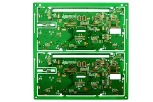
Plugged with Epoxy Resin Multilayer PCB: A Comprehensive Overview
Product Profile
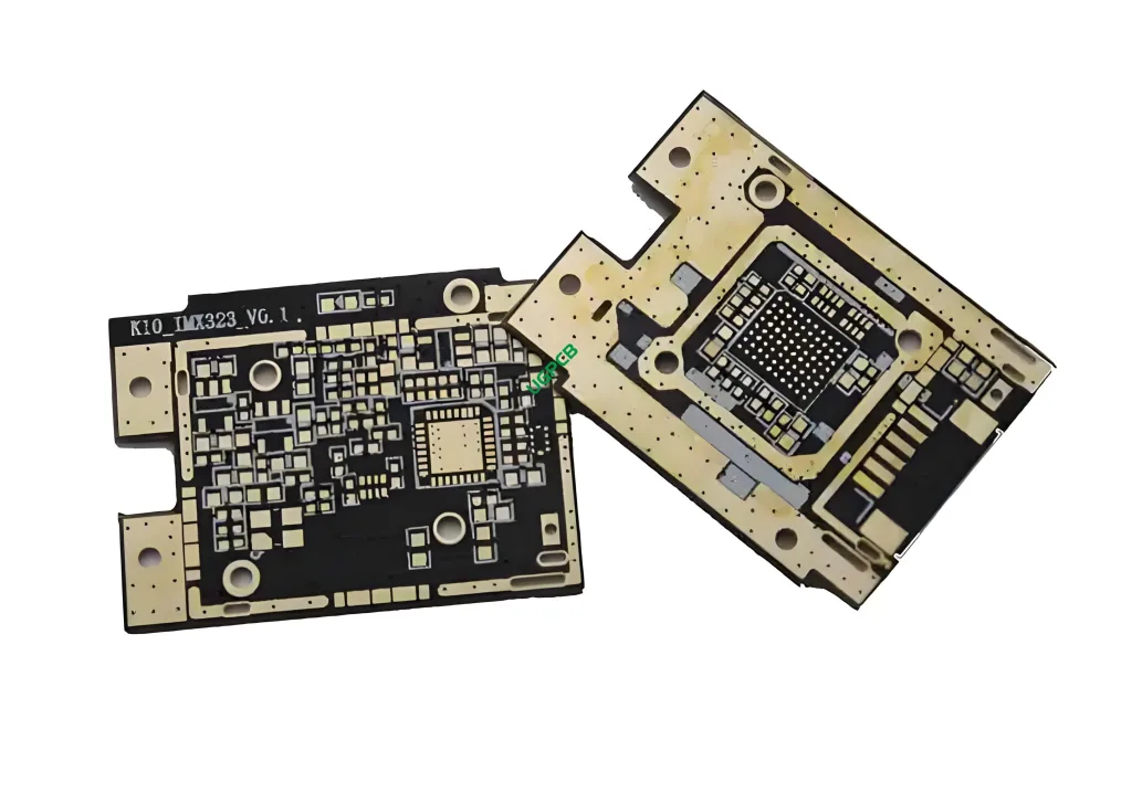
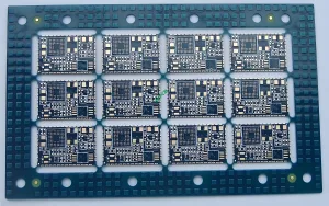
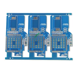
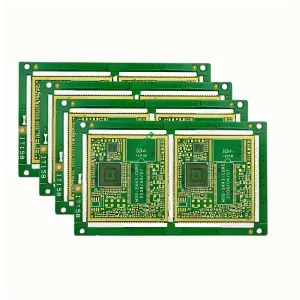
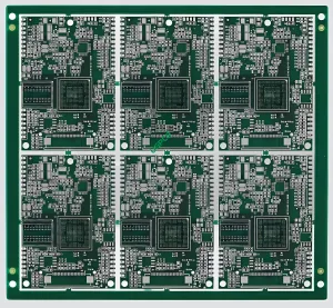
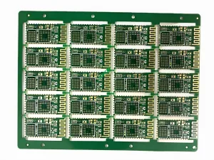
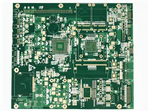
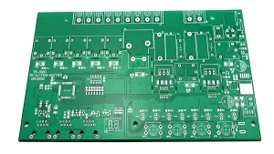
The Plugged with Epoxy Resin Multilayer PCB is a high-performance electronic component designed for complex circuitry applications. This PCB stands out due to its use of epoxy resin plugging, which enhances its durability and reliability.
Definition
A Plugged with Epoxy Resin Multilayer PCB refers to a printed circuit board (プリント基板) that features multiple layers of conductive and non-conductive materials, with epoxy resin used to fill through-holes. This technique ensures robust mechanical support and improved electrical performance.
設計要件
The design specifications of this PCB are meticulously crafted to meet high standards:
- 材料: Premium FR4, known for its excellent thermal and electrical properties.
- レイヤー: Eight layers, allowing for intricate circuit designs and compact form factors.
- 色: Available in Green and White, offering aesthetic flexibility.
- 仕上がり厚さ: 1.2mm, providing a balance between structural integrity and space efficiency.
- 銅の厚さ: 1オズ, ensuring reliable electrical conductivity.
- 表面処理: イマージョンゴールド, enhancing solderability and corrosion resistance.
- 最小トレース/スペース: 4ミル(0.1mm), allowing for fine detailing and high-density layouts.
作業原則
This PCB operates by facilitating the flow of electrical signals through its multilayer structure. The epoxy resin plugging helps in maintaining signal integrity by preventing short circuits and reducing electromagnetic interference (EMI).
アプリケーション
The Plugged with Epoxy Resin Multilayer PCB is widely used in:
- High-Performance Electronics: Such as advanced computing systems and telecommunications equipment.
- Automotive Industry: For engine control units and other critical systems.
- Aerospace and Defense: Where reliability under extreme conditions is crucial.
- 医療機器: Ensuring precision and reliability in diagnostic and therapeutic equipment.
Types and Classification
This PCB can be classified based on several criteria:
- By Technology: Combination of SMD and THD technologies.
- アプリケーションによって: General purpose or specific industries like automotive, 航空宇宙, and medical.
- レイヤーカウントごとに: Eight layers, suitable for complex circuitry.
材料構成
Constructed primarily from FR4, this PCB material offers:
- Superior thermal stability
- High mechanical strength
- Excellent electrical insulation properties
Performance Metrics
Key performance indicators include:
- Signal Integrity: Maintained through careful layout design and impedance matching.
- Reliability: Ensured by rigorous testing protocols and quality control measures.
- 互換性: With a wide range of electronic components and systems.
Structural Features
The PCB’s structure comprises:
- Multilayer stackup for enhanced signal integrity
- Precision-etched traces and spaces for fine circuitry
- Robust through-hole plating for durable mechanical connections
Distinctive Traits
Notable characteristics include:
- Versatility in mounting options (SMD and THD)
- High signal-to-noise ratio due to optimized layout
- Resistance to environmental factors such as humidity and temperature variations
Production Workflow
製造プロセスにはいくつかの段階が含まれます:
- Design and Layout: Using advanced CAD software to create precise schematics.
- 材料の準備: Cutting FR4 sheets to size and cleaning them thoroughly.
- エッチング: Applying etchant to remove unwanted copper from the board.
- メッキ: Immersing the board in a gold bath for surface finishing.
- Assembly: Soldering surface mount and through-hole components accurately.
- テスト: Conducting functional tests to ensure compliance with specifications.
- 品質管理: Final inspection for defects and performance validation.
Use Cases
Typical scenarios where this PCB finds application include:
- Advanced Computing Systems
- Automotive Engine Control Units
- Aerospace Communication Systems
- Medical Diagnostic Equipment
要約すれば, the Plugged with Epoxy Resin Multilayer PCB represents a cutting-edge solution for demanding electronic applications. Its unique combination of advanced materials, meticulous design, and robust manufacturing processes ensures unparalleled performance and reliability across various industries.
 UGPCBのロゴ

