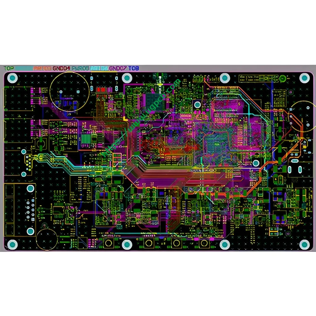
RFプリント回路基板の設計 名前: RFプリント回路基板の設計 設計可能なレイヤー: 1-32 レイヤー 最小ライン幅とライン間隔: 3ミル 最小レーザーアパーチャ: 4ミル 最小機械的開口: 8ミル 銅箔の厚さ: 18-175cm (標準: 18CM35CM70cm) 皮の強度: 1.25N/mm 最小パンチングホールの直径: 片側: 0.9mm/35mil 最小穴の直径: 0.25mm/10mil 開口耐性: ≤φ0.8mm±0.05mm 穴の耐性: ±0.05mm お問い合わせを送信 すぐに見積もりを取得 製品詳細 RF PCBの定義 通常、RF PCBを中程度から非常に高い周波数で動作するように設計された印刷回路基板として定義できます。. RF PCBの周波数範囲 したがって, 100MHzを超える高周波プリント回路基板は、無線周波数印刷回路基板です (UGPCB). 実際の参照周波数範囲 しかし, RF PCBに関しては (UGPCB), 実際の基準周波数範囲は通常、300MHz以上です. マイクロ波PCB 2GHzを超えるRF PCBは、マイクロ波PCBと呼ばれます. 共有: フェイスブックツイッターリンクトインワッツアップ 前へ: コンシューマーエレクトロニクスRF PCB設計 次: 通信剛性RF PCB設計 関連製品 医療スキャナーRF PCB設計 自動車多層RF PCB設計 通信剛性RF PCB設計 コンシューマーエレクトロニクスRF PCB設計 人気の製品 レーダー基板 ロジャース基板 ISOLA 370HR 基板 テフロン高周波基板 12L3+N+3 HDIボード HDI マウスバイト PCB メーカー | 高密度相互接続ボード