Single-sided PCB Overview
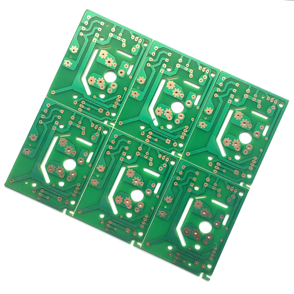
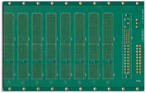
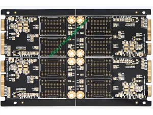
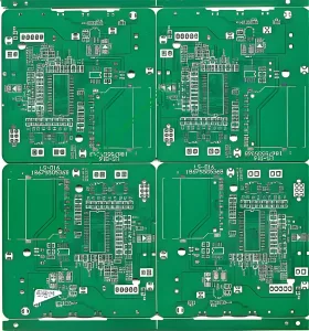
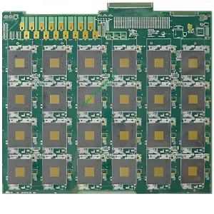
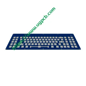
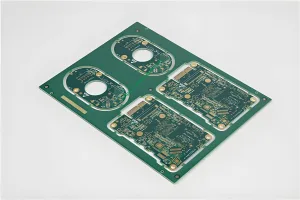
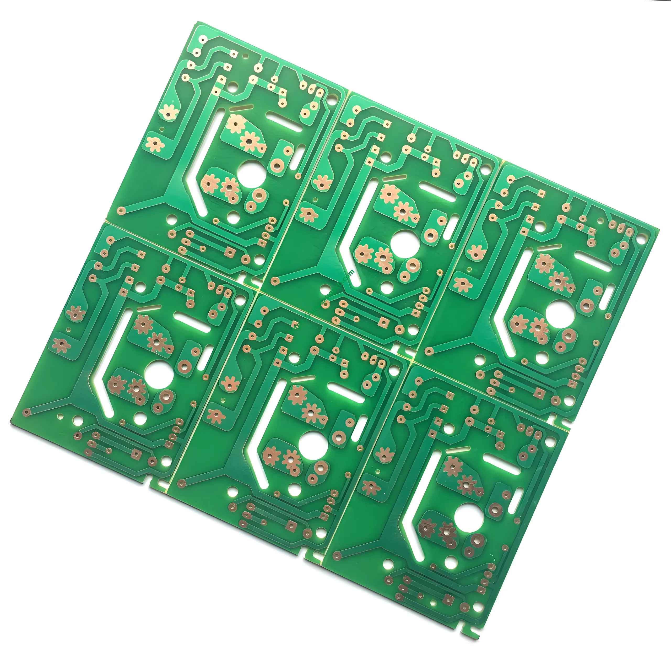
The Single-sided PCB is a fundamental component in electronic manufacturing, offering a simple yet effective platform for the assembly of electronic components. It features a single layer of conductive copper circuitry etched onto a non-conductive substrate, making it ideal for a range of applications where complexity is not a primary requirement.
材料構成
The Single-sided PCB is crafted from various materials to cater to different needs:
- CEM-1: Combines paper and epoxy resin for cost-effectiveness and moderate durability.
- CEM-3: Utilizes glass fiber and epoxy resin for enhanced mechanical strength and electrical insulation.
- FR-4: Known for its flame retardant properties and high glass transition temperature, suitable for demanding applications.
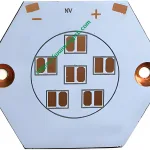
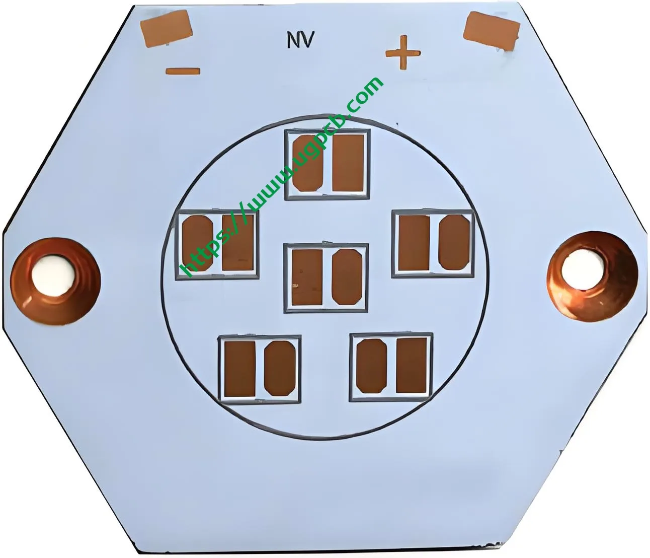
- アルミニウム (アル): Offers exceptional thermal conductivity, making it ideal for heat dissipation in high-power circuits.
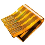
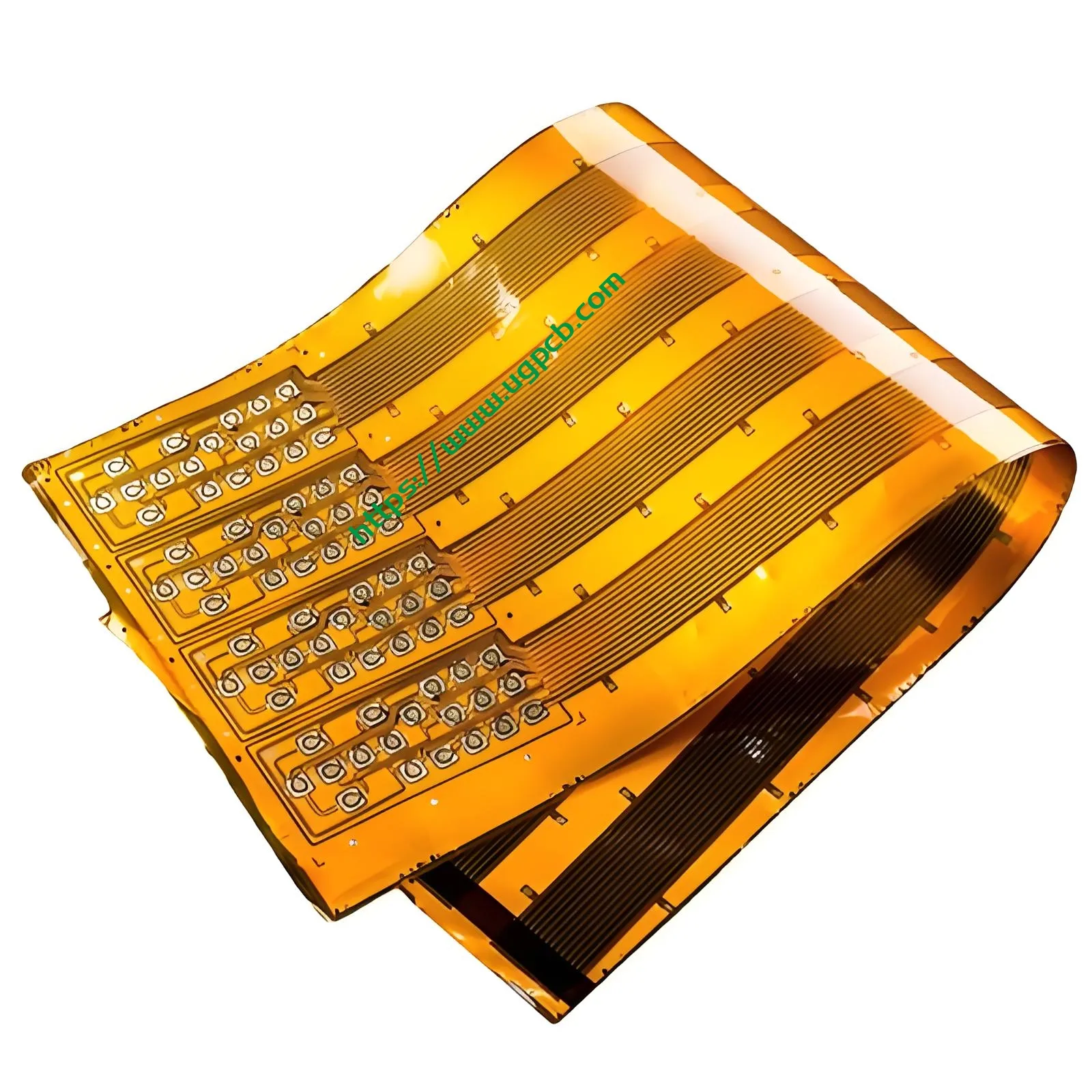
- ポリイミド (PI): Provides flexibility and durability, suitable for applications requiring bending or conformability.
性能特性
These boards are designed with specific performance attributes:
- Layer Configuration: 1層, simplifying the design and manufacturing process.
- カラーオプション: Available in white, 黒, blue, or green, allowing for aesthetic customization.
- 厚さ: Finished thickness ranges from 0.6mm to 1.6mm, accommodating various component heights and packaging requirements.
- 銅の厚さ: Copper thickness of 0.5OZ to 2OZ supports various current carrying capacities and circuit densities.
構造設計
構造的に, the Single-sided PCB comprises:
- Base Material: The substrate that supports the copper circuitry.
- 銅箔: Etched to form the circuit pattern.
- Surface Finish: OSP (Organic Solderability Preservative) treatment ensures good solderability and protects the copper from oxidation.
特徴的な機能
Key features that distinguish Single-sided PCBs include:
- 最小トレース/スペース: Minimum trace and space of 12mil enable high-density routing, crucial for compact designs.
- 表面処理: OSP coating ensures reliable soldering and long-term circuit integrity.
- 多用途性: Suitable for both prototype development and low-volume production runs.
Production Workflow
The production of Single-sided PCBs involves several stages:
- Design and Layout: Circuit diagrams are designed and laid out using CAD software.
- 材料の準備: The chosen substrate and copper foil are prepared.
- Circuit Etching: The copper foil is etched away to form the circuit pattern.
- 掘削: Holes are drilled for component mounting and interconnection.
- Surface Finish: OSP coating is applied to protect the copper.
- 品質管理: Boards undergo rigorous testing to ensure they meet specifications.
- Packaging and Shipment: Boards are packaged and shipped to customers.
アプリケーションシナリオ
Single-sided PCBs are widely used in:
- Educational Kits: Simple circuits for teaching and learning electronics.
- Prototyping: Early-stage development of electronic devices.
- Low-Complexity Devices: Gadgets and appliances that do not require multi-layer complexity.
- DIY Projects: Hobbyist and maker projects requiring cost-effective and straightforward PCBs.
By understanding the material composition, performance characteristics, structural design, distinctive features, production workflow, and application scenarios of Single-sided PCBs, one can appreciate their versatility and essential role in the electronics industry.
 UGPCBのロゴ

