
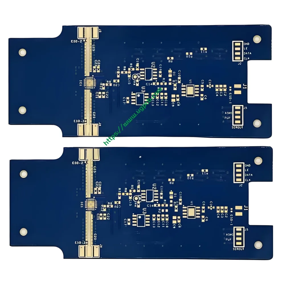
導入
5G通信では, マイクロ波レーダー, 高速データ伝送, 信号の完全性と伝送速度がデバイスの成功を決定します. 標準 プリント基板材料 FR4 のように、誘電損失により高周波で信号が減衰することがよくあります。. これらの要求の厳しいアプリケーション向け, を備えた回路基板が必要です “ゴールデンミディアム” - テフロン基板. プロフェッショナルとして PCBメーカー, UGPCB は、高精度テフロン PCB を提供します。 2 レイヤーへ 34 高度な製造プロセスを使用したレイヤー.

テフロン基板とは?
テフロン基板 を指します プリント基板 ポリテトラフルオロエチレン製 (PTFE, 一般的にテフロンとして知られています) ラミネート材. 非常に安定した化学的および電気的特性により、, この材料は、周波数性能が重要な高周波電子機器で理想的に機能します。.
コア材料と性能パラメータ
テフロンの卓越した高周波性能は、その独特の物理的および電気的特性に由来しています。. UGPCB は、これらのコア仕様を備えたテフロン PCB を製造しています:
-
誘電率 (DK): 2.0 – 3.5. この低い Dk により、広い周波数範囲にわたって安定した値で高速信号伝播が保証されます。.
-
損失係数 (Df): 極めて低い (通常は以下 0.002). Df は信号損失を測定します。値が低いほど、信号の完全性が向上します。. UGPCB は高周波性能を保証するために材料 Dk/Df の厳格な受入検査を実施します.
-
レイヤー: 2 レイヤー – 34 レイヤー. シンプルな両面基板が必要な場合も、複雑な 34 層多層 PCB が必要な場合も, UGPCB のプロフェッショナルなラミネートプロセスは、.
-
板厚: 0.1mm – 12mm, 多様なパワーと構造要件に対応.
-
銅の厚さ: ベース銅 0.5オンス, 完成した銅の厚さ 1オンス, 電流容量とライン精度のバランスをとる.
-
表面仕上げ: イマージョン ゴールドまたは ISIG. これらの平坦な仕上げは、高周波信号の表皮効果をサポートし、損失を最小限に抑えます。.
科学的分類
-
ベース素材によって: 特殊材料PCB (有機樹脂部門 – PTFE系)
-
周波数別: 高周波マイクロ波PCB
-
構造によって: 多層リジッドPCB (ハイブリッド構造を含む)
-
アプリケーションによって: RF/マイクロ波回路基板
動作原理と主要な設計ポイント
マイクロ波高周波回路において, 信号の波長は伝送中に非常に短くなる. テフロン基板 超低誘電率と損失を利用して、正確にインピーダンス制御された配線内に電磁波を閉じ込めます。 (通常 50 または 75 オーム), 反射と減衰を最小限に抑える.
設計上の重要な考慮事項
UGPCB テフロン PCB を設計する場合、2 つの要素が最も重要です:
-
高いRFライン精度: アンテナ給電線やマイクロストリップなどの高周波配線には、厳密な幅と間隔の制御が必要です. 小さな誤差がインピーダンスの不整合を引き起こす. UGPCB は高精度のエッチングを使用して、正確な RF ラインの形成を保証します.
-
Dk/Df 材料の選択: 動作周波数に一致する Dk 値を持つ材料を選択してください. UGPCB は、Rogers や Taconic シリーズなどの材料の選択と検証に役立ちます.
製品の分類と構造
テフロン PCB は構造と材料の組み合わせによって分類されます:
-
純粋なテフロン PCB: 完全に PTFE ラミネートで作られています. これらは最大限の安定性を提供しますが、コストが高くなります. PTFE の柔らかい性質により、, 多くの場合、特別な器具が必要になります.
-
ハイブリッドテフロン基板: コストと機械的強度のバランスをとるため, テフロン+FR4ハイブリッド構造 うまくいきます. 高周波層にはテフロンを使用し、その他の層にはFR4を使用. これには、さまざまな熱膨張係数に適合する高度なラミネート加工が必要です. UGPCB にはハイブリッド ラミネートの豊富な経験があります.
UGPCB の製造プロセスと品質管理
高品質のテフロン PCB には厳格なプロセス管理が必要です:
-
前処理: テフロンは表面エネルギーが低いため、ビアホール内の銅の密着性を高めるために、穴あけ前にプラズマまたはナトリウムナフタレン処理が必要です。.
-
掘削: PTFE の柔らかさとガラス含有量により、FR4 とは異なる穴あけパラメータが必要になります. 専用ビットを使用し、バリや穴壁の荒れを防ぎます.
-
メッキ: 特殊発動後, 穴壁が強力な銅接続を実現.
-
パターン転写: クリーンルーム条件での高精度のアライメントと露光により、RF ラインの精度が保証されます.
-
エッチング: サイドエッチングを厳密に管理し、配線の直方性を維持, 高周波インピーダンスにとって重要.
-
品質検査: 完成品はIPC-A-600による外観検査を受け、 100% 電気試験, ミーティング IPC6012 クラス II またはクラス III 要件.
主要なアプリケーション
優れたマイクロ波特性を備えています, UGPCB テフロン PCB は次の分野に使用されます:
-
通信インフラストラクチャ: パワーアンプ, アンテナシステム
-
衛星通信: LNB, トランスポンダーモジュール
-
自動車レーダー: 77GHzミリ波レーダー, 衝突回避システム
-
航空宇宙 & 防衛: ナビゲーション装置, 電子的対策
-
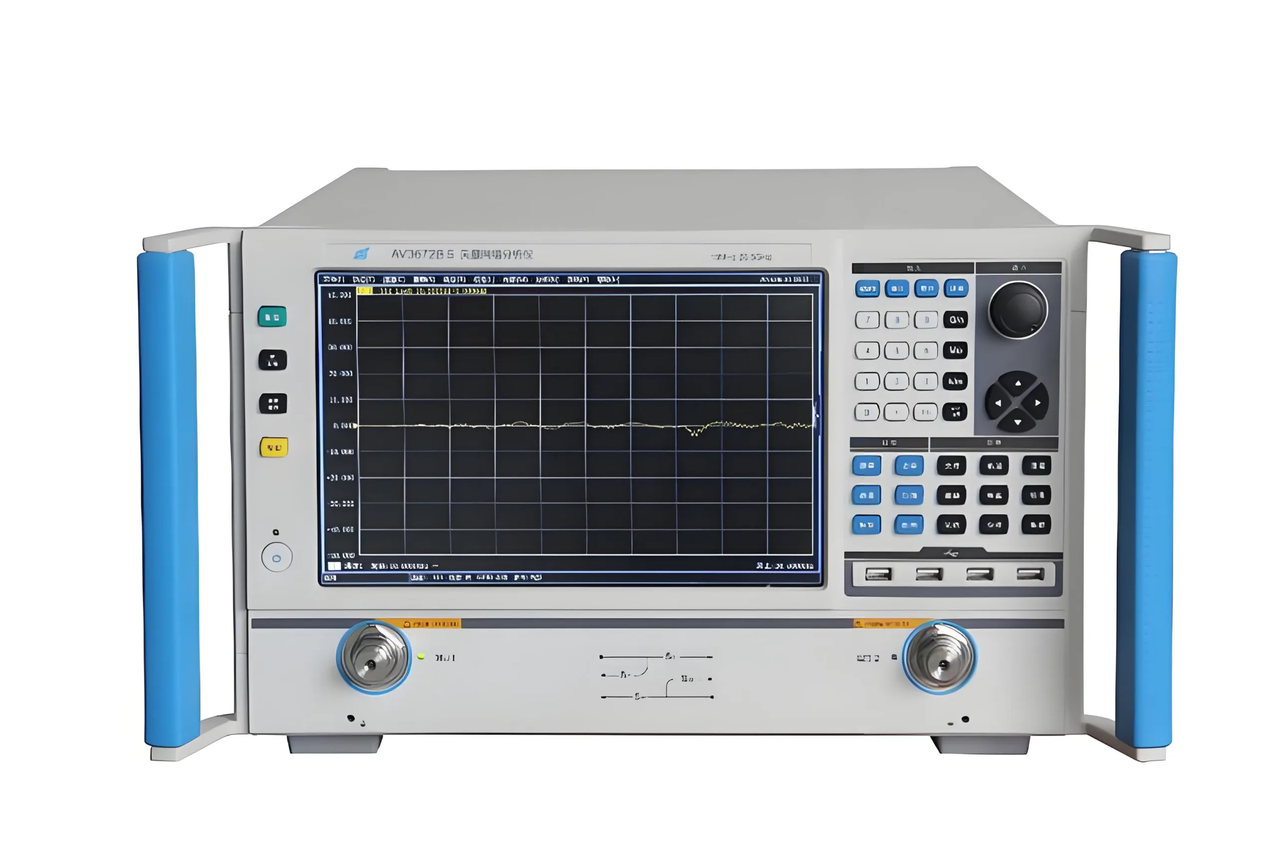
試験機器: ネットワークアナライザ, 高周波プローブ, テストフィクスチャ
テフロン PCB に UGPCB を選択する理由?
-
高周波の専門知識: Dk/Df が信号に与える影響を理解しています. 素材の選択から生産まですべてを管理.
-
高多層化能力: まで対応いたします 34 複雑なデザインに対応するテフロン層とハイブリッド構造.
-
精密フォーカス: 当社は、インピーダンス許容差が ±5% 以内またはそれより厳しい高精度 RF ラインを専門としています。.
-
品質認証済み: 当社は IPC6012 クラス II/III 規格に厳密に従っています, 信頼できる品質保証を提供します.
今日行動を起こしてください
優れた電子レンジ機器は優れた製品から始まります テフロン基板. 安定性が必要な場合, 信頼性のある, 高周波アプリケーション向けの高性能 PCB ソリューション, UGPCB は信頼できるパートナーです.
材料の制限によってデザインの可能性が制限されないようにする.
[PCB 設計ファイルを送信する (ガーバー) と要件. 今すぐ UGPCB から専門的な見積もりと DFM 分析を入手してください!]


