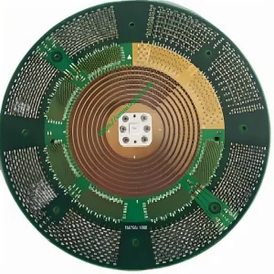
材料構成
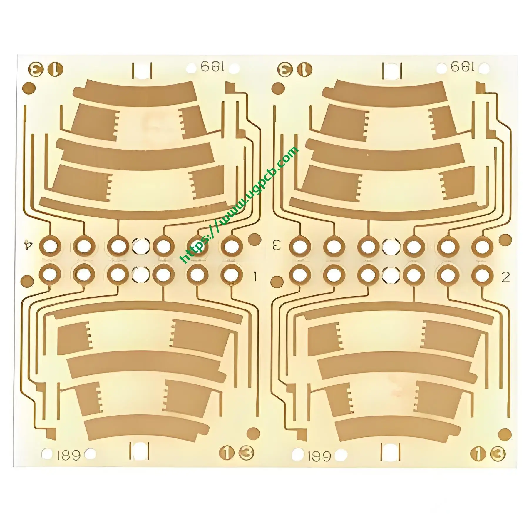
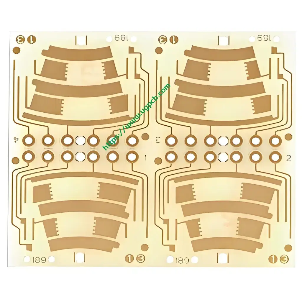
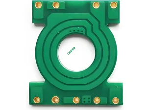
The Throttle Door Sensor PCB is crafted using high-quality ceramic PCB material. This selection ensures robustness, 耐熱性, および電気絶縁, making it ideal for applications requiring reliability and durability under demanding conditions.
Performance Capabilities
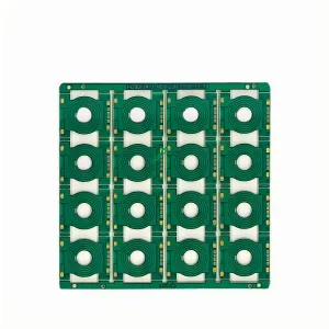
Boasting a 2-layer PCB design, the Throttle Door Sensor PCB offers superior circuit integration and compactness. The white substrate not only provides a clean aesthetic but also enhances visibility and inspection during manufacturing and maintenance. With a finished thickness of 1.6mm and a copper thickness of 1OZ, it balances strength and conductivity, ensuring efficient signal transmission and robust component mounting.
Distinctive Characteristics
The standout feature of this PCB is its special process—gold-plated PCB combined with a ceramic substrate PCB. Gold plating enhances corrosion resistance, improves electrical conductivity, and ensures smooth soldering processes, which are crucial for maintaining the sensor’s precision and longevity. The ceramic substrate further adds thermal stability, making the PCB resilient to temperature fluctuations often encountered in automotive throttle systems.
Production Workflow
The production of the Throttle Door Sensor PCB involves several meticulous steps:
- Design and Layout: Expert engineers design the PCB layout, ensuring optimal circuit placement and routing to minimize interference and maximize performance.
- 材料の準備: High-grade ceramic substrate and copper foil are prepared according to specifications.
- Manufacturing: The ceramic substrate undergoes drilling, copper etching, and layer lamination to form the 2-layer PCB structure.
- 金メッキ: The PCB surfaces are then gold-plated to enhance conductivity and corrosion resistance.
- 品質管理: Rigorous testing ensures that each PCB meets stringent quality standards before moving to the next stage.
- Final Assembly: Components are mounted, and the PCB is tested again in its complete form to guarantee reliability.
アプリケーションシナリオ
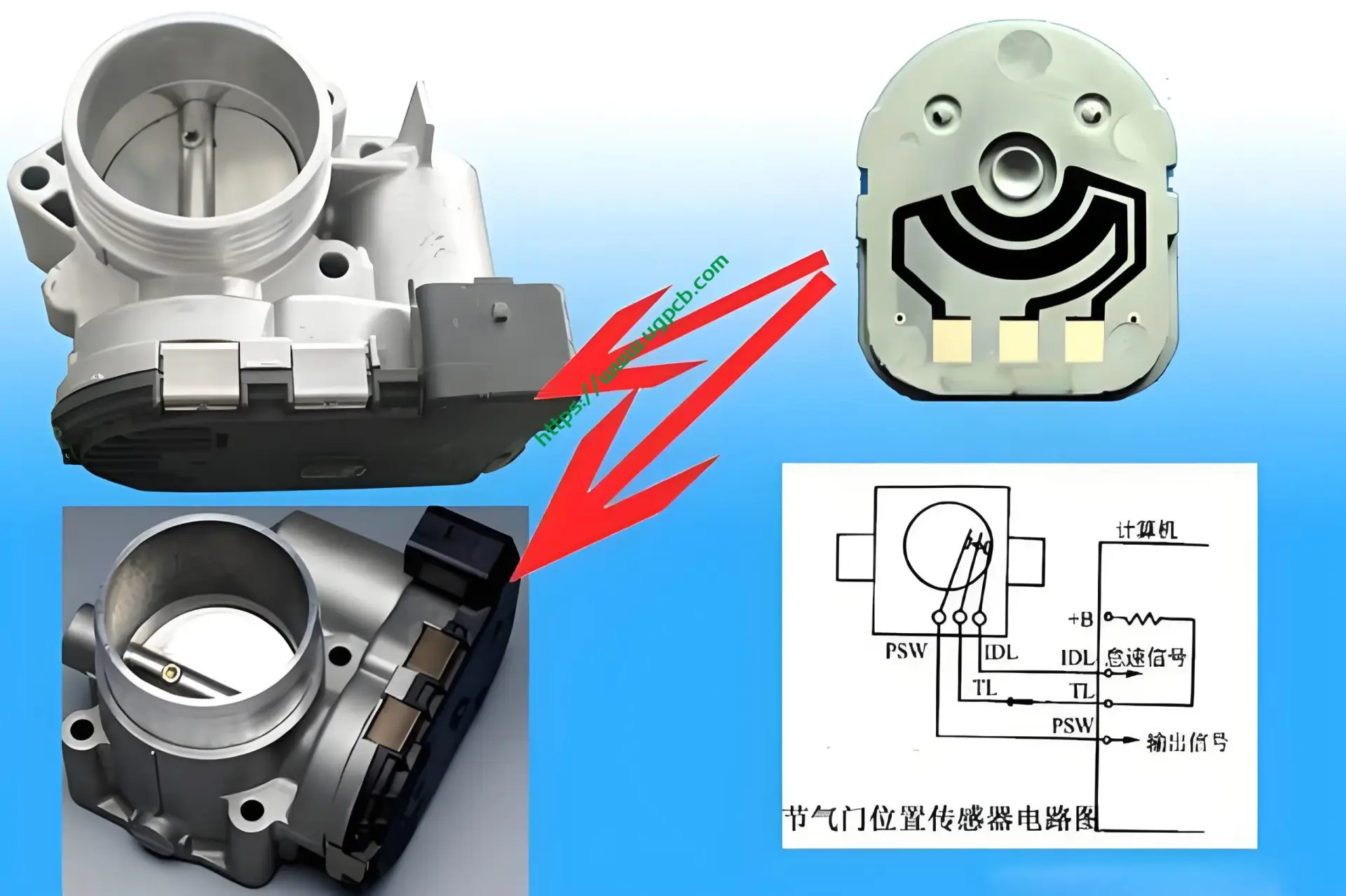
The Throttle Door Sensor PCB is primarily used in automotive throttle systems, where precision and reliability are paramount. It serves as a critical component in throttle position sensors, enabling accurate monitoring and control of engine throttle input. By integrating seamlessly into modern vehicle electronics, it helps maintain smooth acceleration, fuel efficiency, and overall driving performance.
This advanced PCB design not only meets but exceeds the expectations for durability, accuracy, and performance in high-stress automotive environments, ensuring a safer and more enjoyable driving experience.
 UGPCBのロゴ

