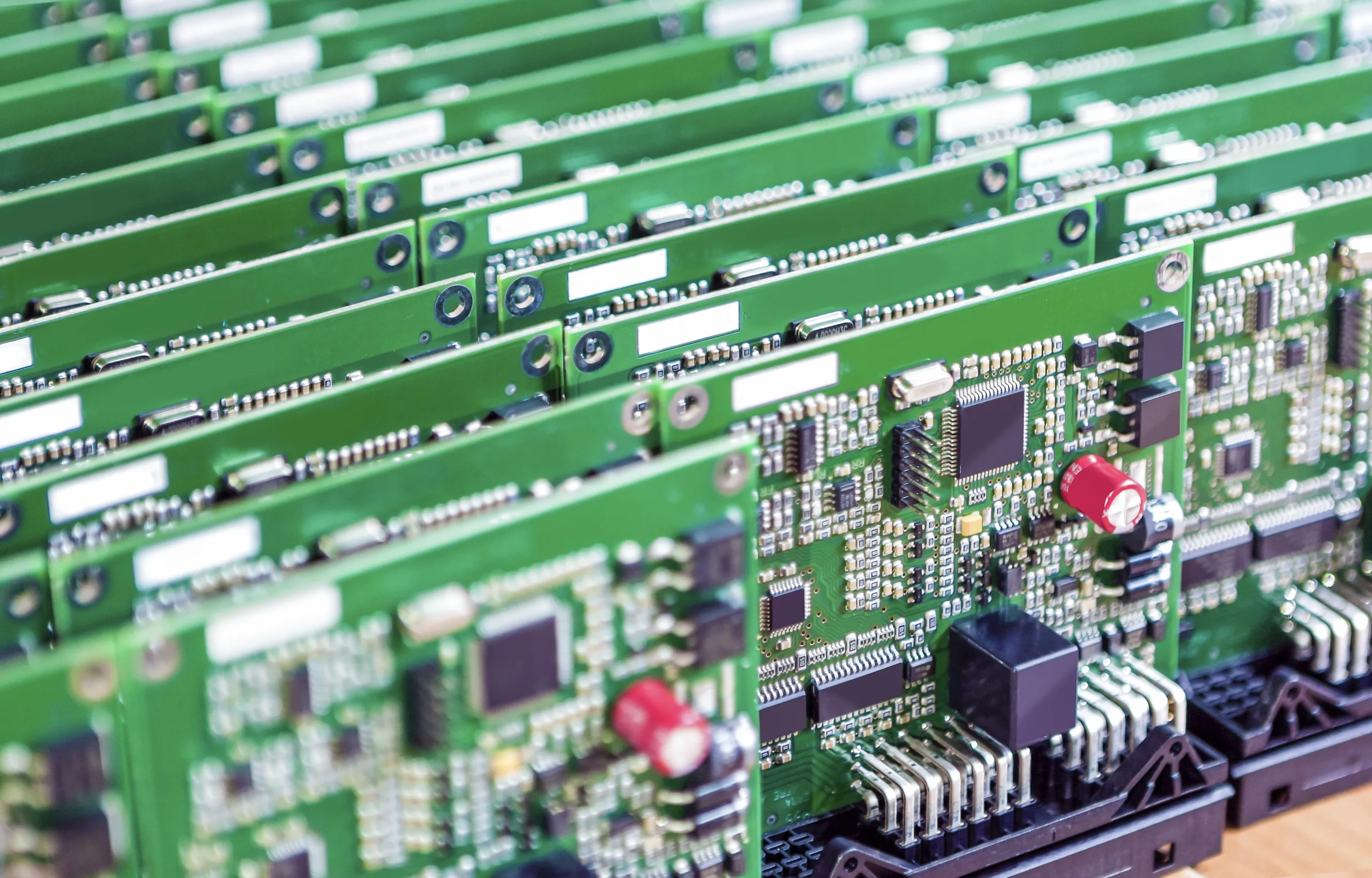
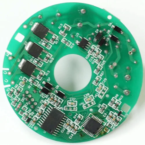
General Information
- Model Number: PCB/PCB Assembly
- Place of Origin: Guangdong, 中国
- Supplier Type: OEM/ODM
Layer and Board Specifications
- 層: 1-20
- 板厚: 0.20mm-4.0mm
- 銅の厚さ: 17.5um-175um (0.5oz-5oz)
Solder Mask and Stencil Cleaning
- Solder mask color: 赤, 黒, blue, 緑, 黄色
- Frequency of stencil cleaning: 1 time/5 to 10 pieces
Surface Treatment Options
- 表面処理: HASL, Lead free HASL, OSP, 金メッキ, イマージョンゴールド
Trace, Line, and Space Specifications
- Min Trace Width: 0.15mm
- Min. Line Spacing: 3 ミル (0.075 mm)
- Min Space Width: 0.15mm
Base Material Options
- Base Material: FR4/CEM-1/CEM-3/Aluminium
Drilling Specifications
- Min Drilling Dia: 0.2mm


