PCBA 표면 실장 조립 과정에서, 다양한 전자 부품이 자주 고장납니다.. 오늘, 3A 선형 레귤레이터의 고장 분석에 대한 사례 연구를 공유합니다., 표면 너머를 살펴보고 결함을 빠르게 식별하는 방법을 설명합니다..
1) Chip failure description: Vin is short-circuited to ground.
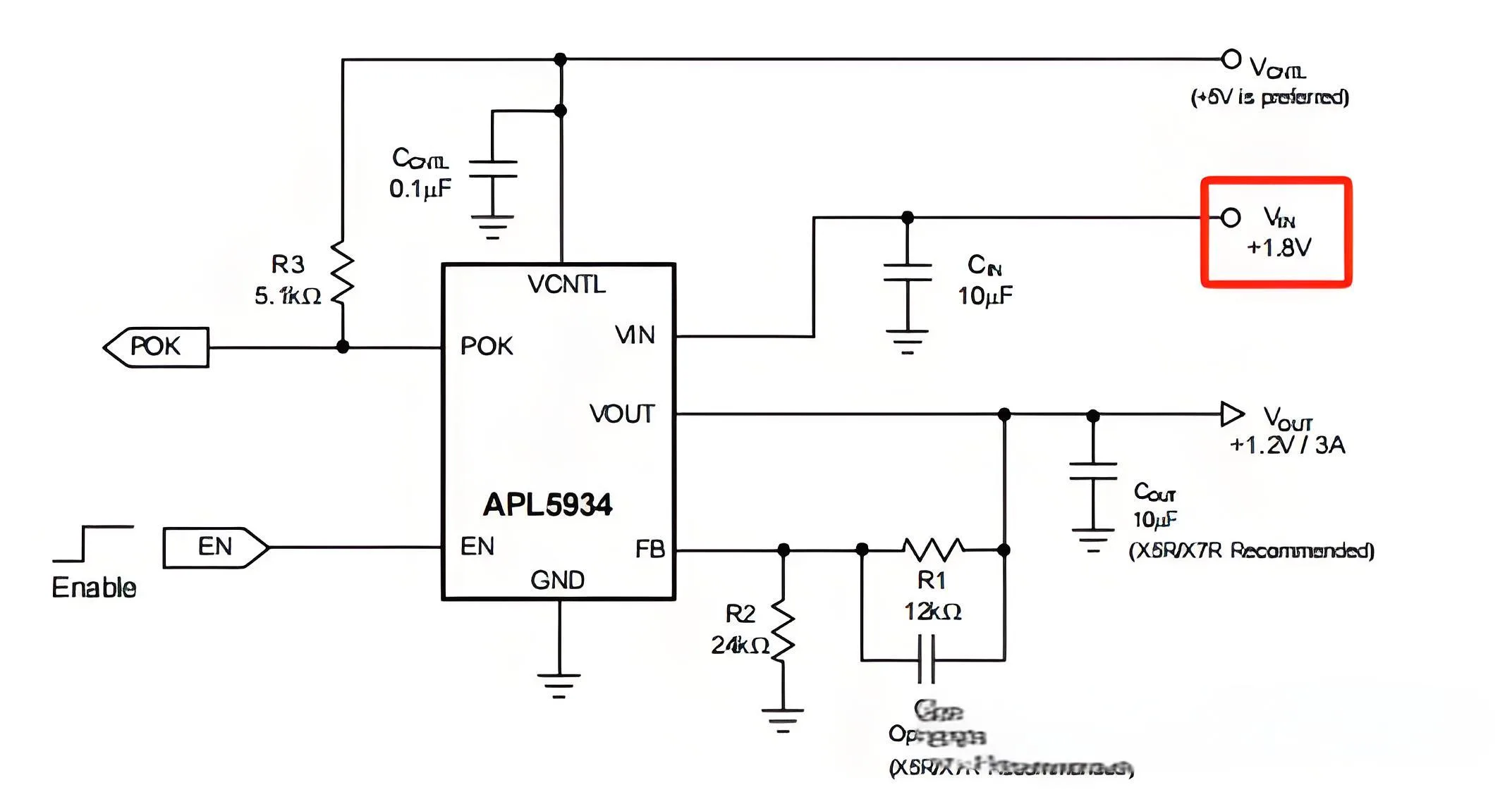
Vin is short-circuited to ground.
2) Device failure analysis: The chip experienced an EOS (Electrical Over-Stress) failure as confirmed by IV testing with Vin short-circuited to ground.
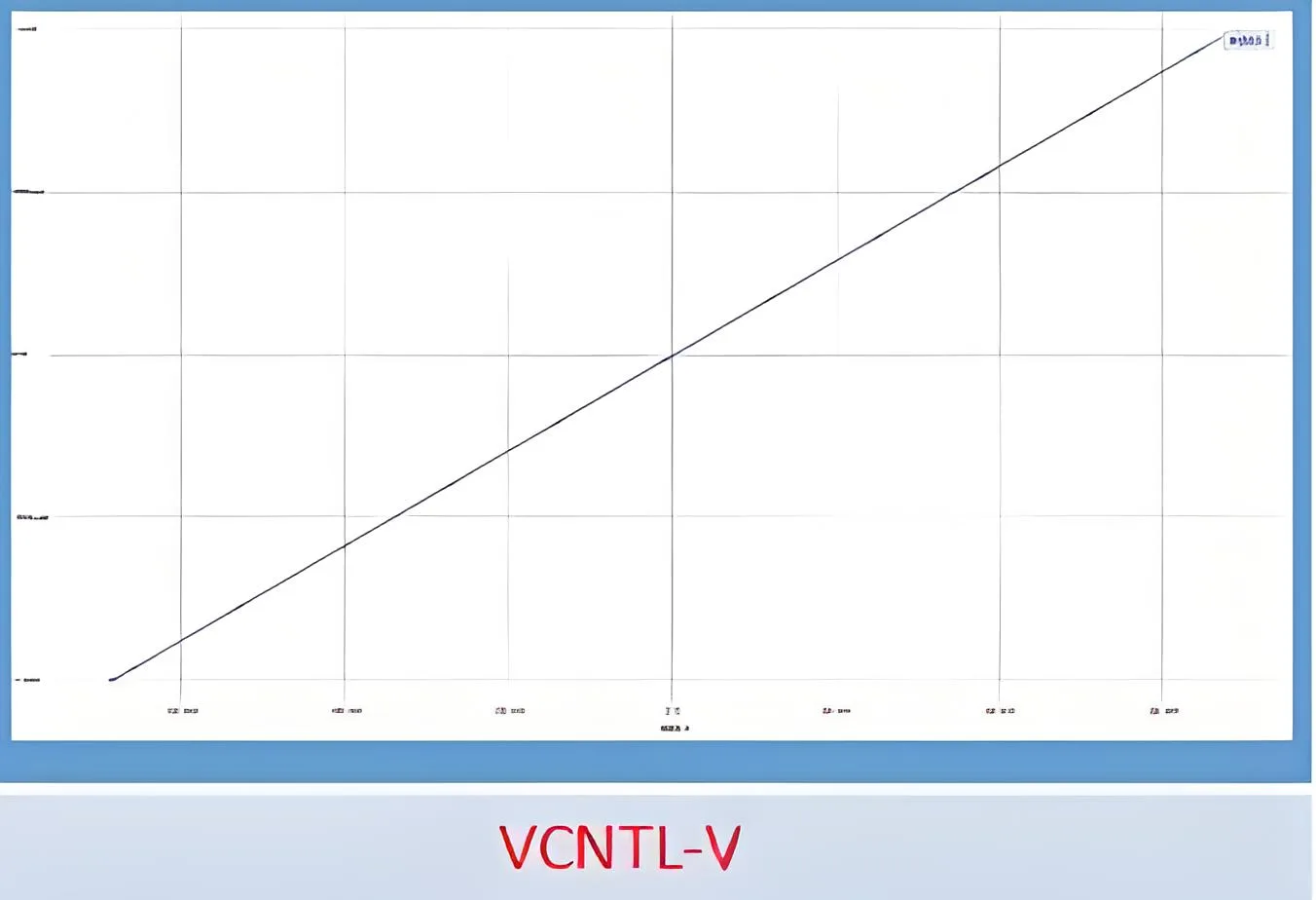
IV test confirms Vin to ground short circuit.
No obvious anomalies were observed in appearance or acoustic scanning, but X-ray revealed suspected burn damage.
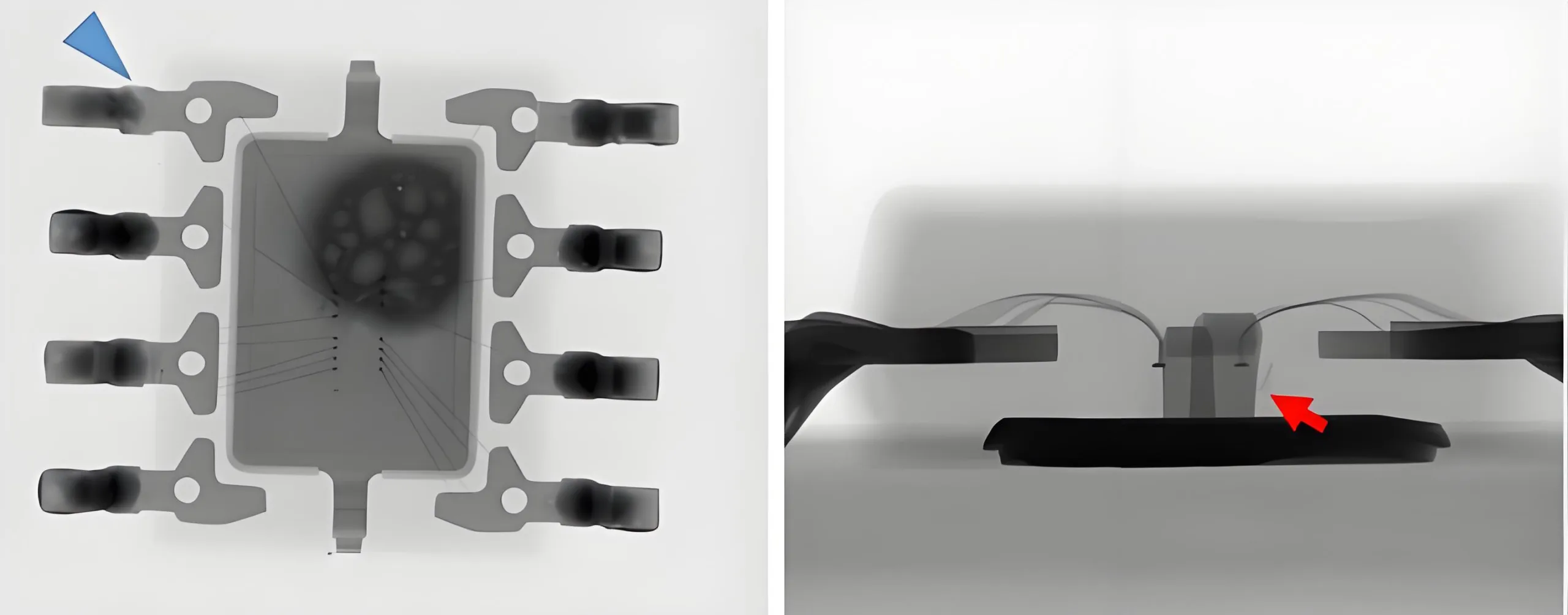
Suspected to have been burned
Upon opening the cover, it was found that the chip’s EOS burnout was most severe at the VCNTL pin rather than Vin.
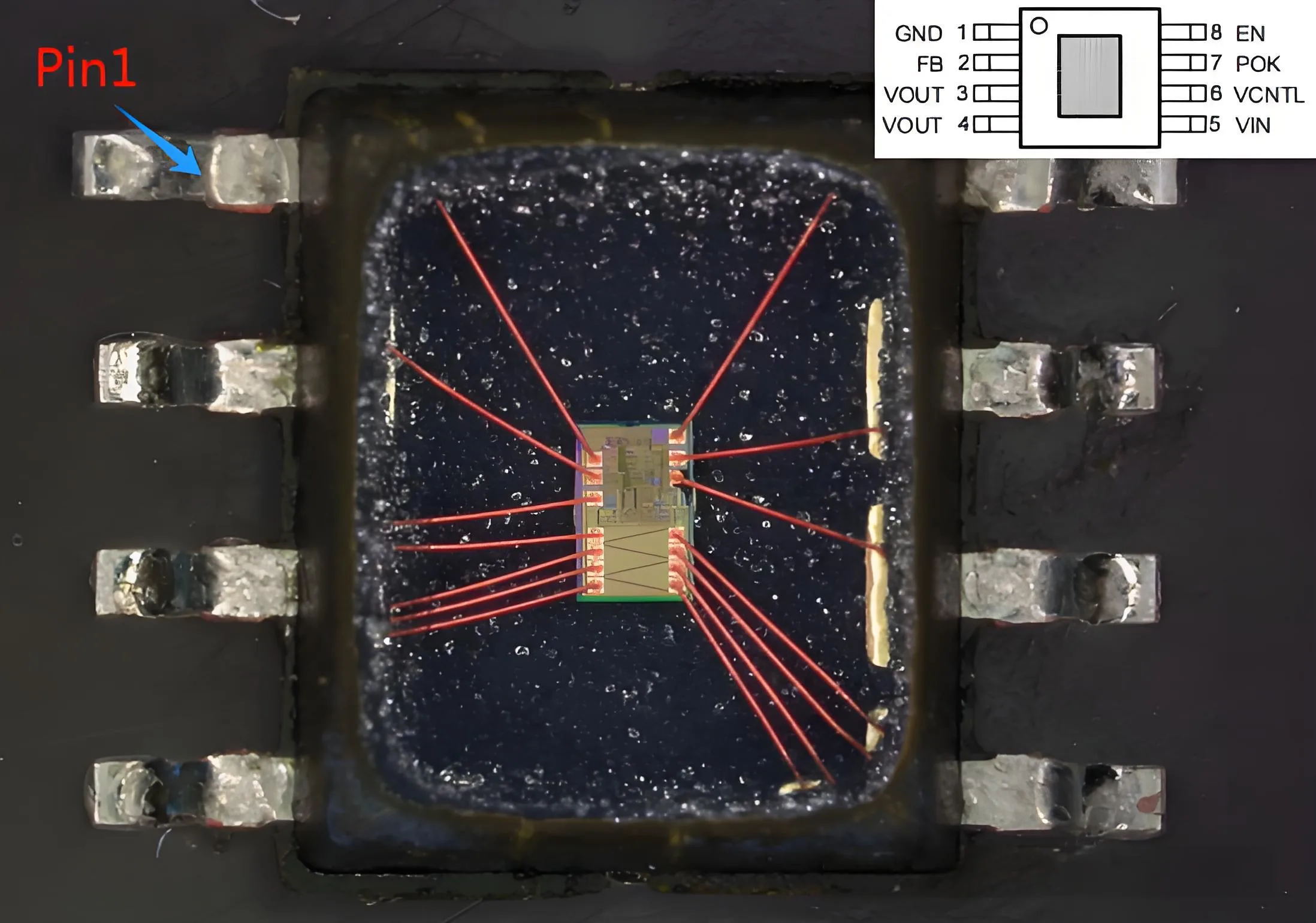
The chip’s EOS has been burned out
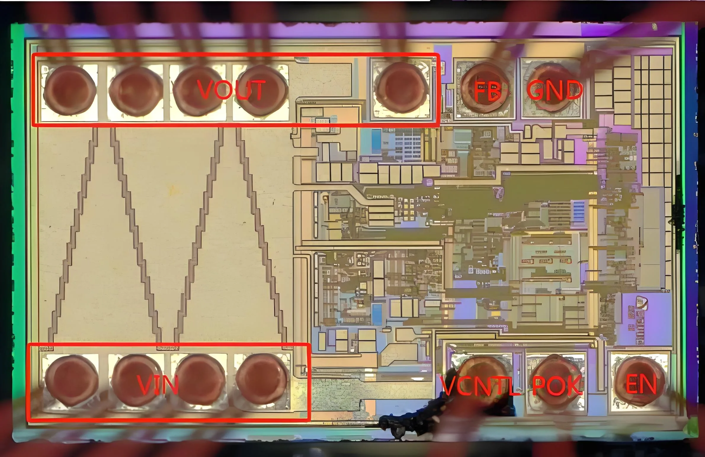
The chip’s EOS has been burned out
3) Root cause analysis: It is suspected that over-voltage stress introduced by VCNTL caused the chip failure. The VCNTL pin is defined as an input pin, which could potentially experience over-voltage stress.
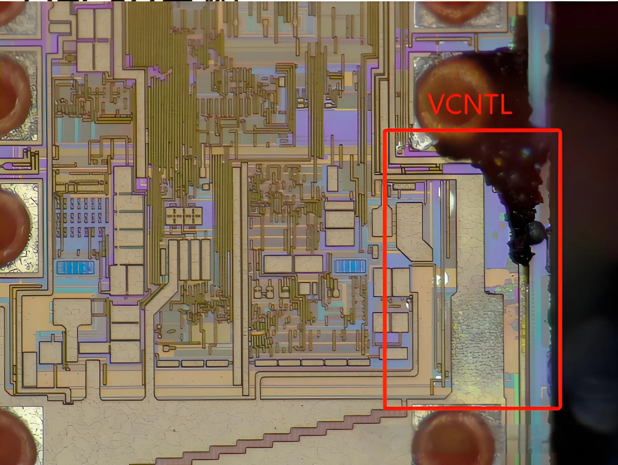
VCNTL introduces excessive electrical stress leading to failure
Further analysis revealed that the metal morphology along the VCNTL-VIN link appeared melted, and measuring the IV between VCNTL and VIN showed a short circuit. 그러므로, the chip failed due to over-voltage stress introduced by VCNTL. Analysis of the chip’s logic block diagram matched the failure phenomenon with its logical function.
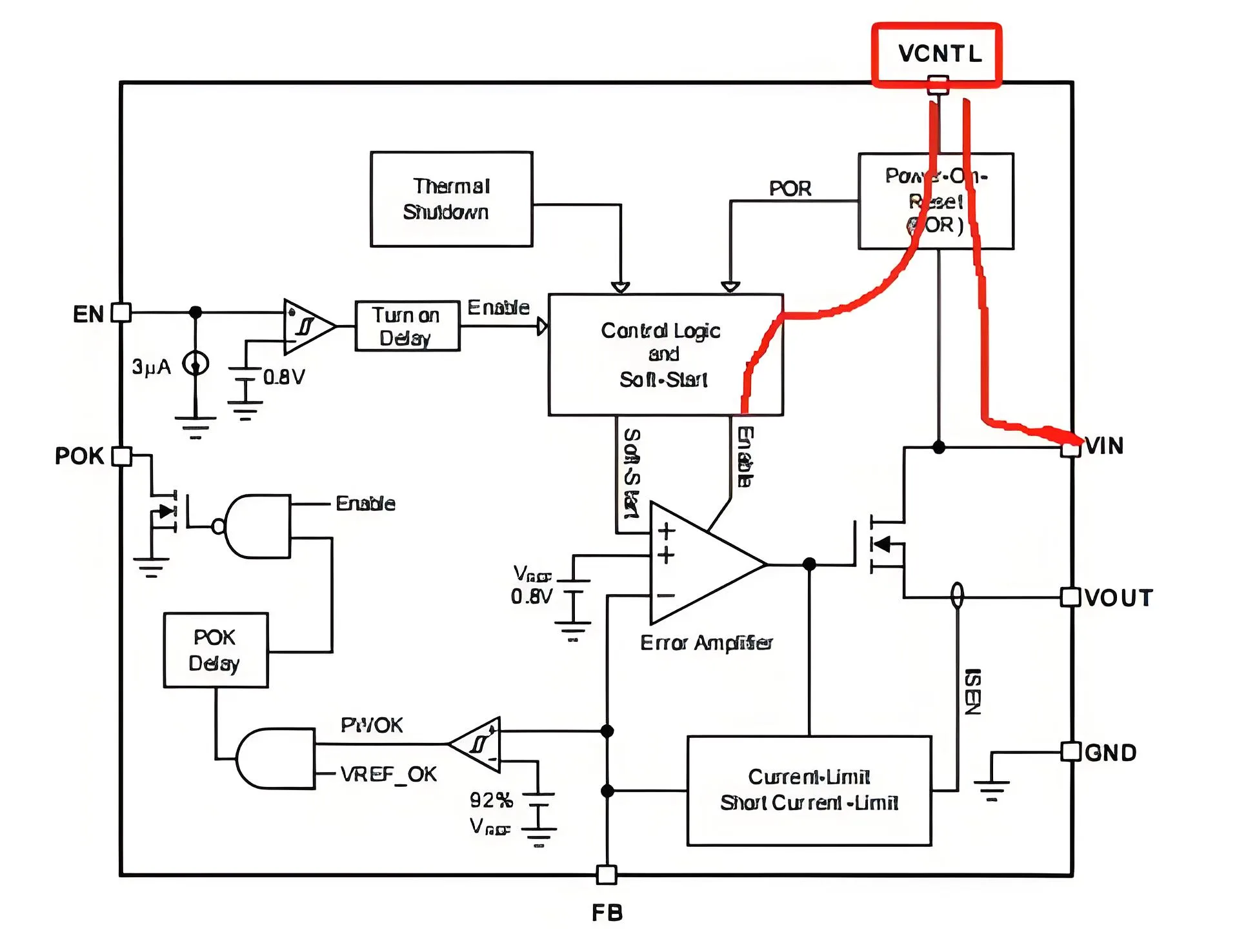
Chip Logic Diagram
Removing the top layer of metal clarified that the chip’s failure was indeed caused by over-voltage stress introduced by VCNTL.
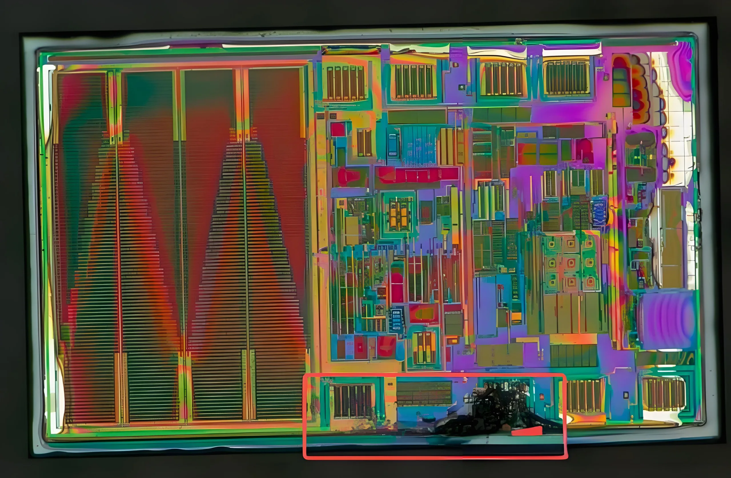
VCNTL introduces excessive electrical stress leading to failure.
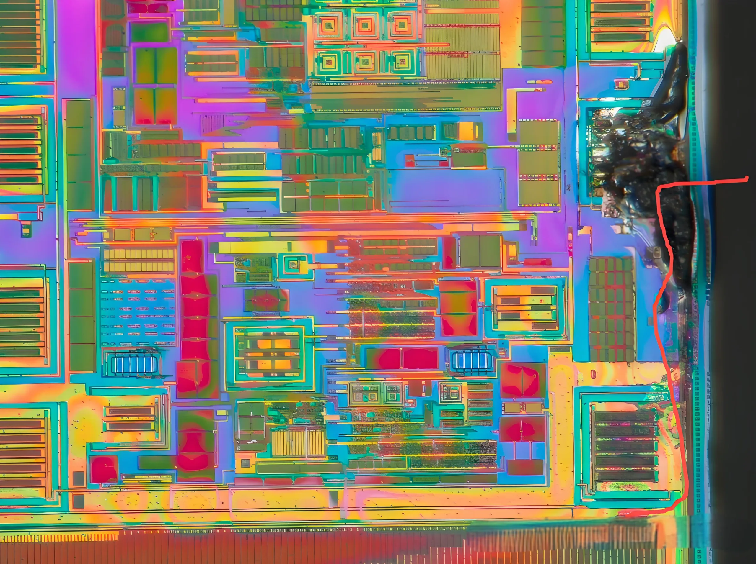
VCNTL introduces excessive electrical stress leading to failure.
4) Board level confirmation: After analysis, it was confirmed that damage to other peripheral devices on the board caused the voltage stress on the VCNTL pin to exceed its specification value. 따라서, this chip was a “victim.”
EOS is the most common phenomenon encountered in failure analysis. Identifying the root cause through EOS failure symptoms is challenging and requires analysts to have clear logical thinking and extensive knowledge.
 UGPCB 로고

