
다층 PCB
UGPCB High-Multilayer PCB Solutions: Driving Innovation in High-Density Electronic Systems through Precision Stacking Technology
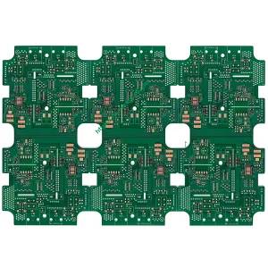
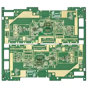
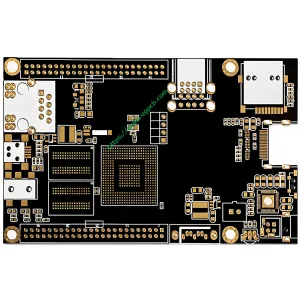
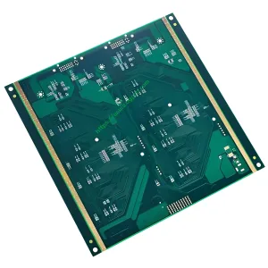
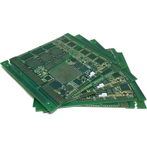
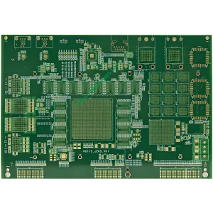
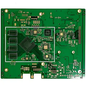
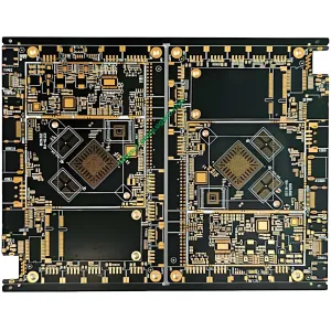
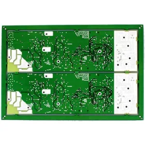
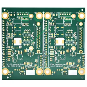
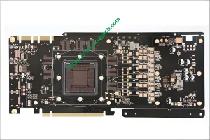
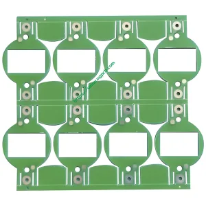
In the era of rapid advancements in 5G communication, AI 서버, and high-end industrial equipment, UGPCB, with over a decade of experience in high-multilayer PCB design, 생산, and PCBA assembly, presents a selection of our multilayer PCB products in the “다층 PCB” section of our corporate website. We delve into how cutting-edge processes and interdisciplinary design capabilities enable us to provide customized solutions for 8-40 layer high-density interconnect boards, 고주파 고속 보드, and HDI PCBs, meeting stringent requirements for signal integrity, 열 안정성, and long-term reliability in harsh environments.
Core Technical Advantages: Setting the Benchmark for High-Multilayer PCB Performance
-
High-Precision PCB Stackup Architecture Design
• Ultra-High Layer Count Capability: Our company has successfully mass-produced 40-layer PCB products with layer-to-layer alignment accuracy of ±25μm (using LDI laser direct imaging technology), supporting 0.1mm microvias, blind/buried vias, and Any-layer HDI.
• Hybrid Material Integration: Flexibly combining materials such as FR-4, 로저스, and MEGTRON®, we optimize Df values to 0.0015@10GHz, reducing insertion loss by 30% compared to traditional stackup solutions.
-
Signal and Power Integrity Assurance
• Full-Band Impedance Control: Based on Ansys SIwave simulations, we achieve impedance tolerances of ±5% for 28Gbps high-speed signals and power plane impedances <2MΩ, meeting PCIe 5.0/USB4 specifications.
• 3D Electromagnetic Shielding: Employing stepped copper foil filling and localized ground isolation techniques, we achieve radiation noise attenuation of >55dB@6GHz, passing FCC Part 15/EN 55032 Class B certifications.
-
Thermal-Mechanical Reliability Enhancement
• CTE Dynamic Balancing Technology: By using Low CTE materials (such as TUC TU-872SLK) in the core layers to match the copper layer expansion coefficients, we ensure no delamination after 1000 thermal cycle tests (-55℃↔125℃).
• High-Thermal-Conductivity Structure Design: Incorporating 2W/mK thermal adhesive and aluminum-based heat dissipation channels, we reduce thermal resistance by 40%, ensuring stable operation of high-power ICs.
Typical Application Scenarios and Technical Parameters
• 5G Base Station AAU Motherboard: 24-layer high-frequency hybrid PCB, combining Rogers RO4835™ and FR-4, achieving insertion loss ≤0.3dB/inch in the n260 frequency band and supporting 256T256R Massive MIMO architectures.
• Data Center GPU Accelerator Card: 32-layer high-speed PCB using MEGTRON®6 material, with 112G PAM4 signal loss <0.8dB/cm, passing OCP Open Compute Standards certification.
• Industrial Automation Main Control Board: 16-layer high-TG thick copper PCB (3oz inner layers/6oz outer layers), capable of continuous operation at 150℃, meeting IEC 61131-2 vibration/shock standards.
Full-Process Services and Certification System
• Collaborative Design Support: Providing Cadence Allegro/PADS stackup simulations, HyperLynx signal integrity analysis, and Valor DFM manufacturability verification.
• Rapid Prototyping Delivery: 5-day sample delivery for 12-layer PCBs, 10-day delivery for 20+ 레이어 HDI 보드, supporting 1-6th order laser via processes.
• Stringent Quality Assurance: 100% compliance with IPC-6012 Class 3 표준, ISO 9001/IATF 16949 certifications, 항공 우주 산업을 다루는 군사 등급의 NADCAP 자격.
UGPCB를 선택 해야하는 이유
-
기술적 깊이: 위에 200 고중도 PCB 특허 기술, 112g 고속/77GHz 밀리미터 웨이브와 같은 최첨단 시나리오를 포함하는 데이터베이스..
-
비용 최적화: 스마트 패널화 체계는 재료 활용을 증가시킵니다 15%, 하이브리드 스택 업 설계는 BOM 비용을 줄입니다 20%-35%.
-
대량 생산 보증: 완전 자동화 된 생산 라인은 ± 2%의 라미네이션 정확도를 달성합니다., 안정적인 수율 속도 >99.2% 대량 주문.
지금 맞춤형 UGPCB 고중도 PCB 솔루션을 받으십시오
아래의 관련 제품을 방문하십시오 “다층 PCB” 공식 웹 사이트의 섹션, 요구 사항을 제출하십시오, 무료 견적 및 기술 지원을받습니다.
 UGPCB 로고
위챗
WeChat으로 QR 코드를 스캔하세요