
4Layers 다층 Bluetooth PCB의 개요
4 층 다층 블루투스 PCB Bluetooth 애플리케이션의 엄격한 요구 사항을 충족하도록 설계된 특수 제품입니다.. 이 유형의 PCB는 신호 무결성이 높습니다, 열 안정성, 신뢰성, 다양한 Bluetooth 지원 장치에 이상적인 선택입니다.

정의
4 층 다층 Bluetooth PCB는 a입니다 인쇄 회로 기판 Bluetooth 모듈의 기능을 지원하도록 특별히 설계되었습니다.. 그것은 여러 층의 전도성과 단열로 구성됩니다 재료, Bluetooth 장치 작동에 필수적인 복잡한 전기 경로 및 연결 제공. 용어 “4-층” 전도성 층의 수를 나타냅니다, ~하는 동안 “다층” 2 개 이상의 전도성 물질이 있음을 나타냅니다..
설계 요구 사항
4 층 다층 Bluetooth PCB를 설계 할 때, 몇 가지 주요 요구 사항을 충족해야 합니다.:
- 재료 품질: 고품질 FR4 재료는 내구성 및 열 안정성에 필수적입니다..
- 레이어 구성: 2 층 디자인은 표준입니다, 신호와 전력의 효율적인 라우팅을 허용합니다.
- 구리 두께: 1OZ의 구리 두께로 적절한 전도성 보장.
- 표면 처리: 침수 금 표면 처리로 연결성과 내식성이 향상되었습니다..
- 추적/공간 차원: 4mil의 최소 트레이스 및 공간 크기 (0.1mm) 정밀한 회로 패턴이 필요합니다..
- 특별한 기능: Half-Hole PCB 설계는 종종 특정 구성 요소 배치 및 납땜 요구 사항을 위해 통합됩니다..
작동 원리
4 층 다층 Bluetooth PCB는 전기 전도도 및 신호 무결성의 원리에 따라 작동합니다.. 전도성 층은 전기 신호의 경로를 형성합니다., 절연층은 이러한 신호 간의 원치 않는 상호 작용을 방지합니다.. 하프 홀 디자인은 더 나은 신호 라우팅을 허용하고 Crosstalk를 줄입니다.. 침지형 금 표면 처리로 우수한 연결성을 제공하고 환경 요인으로부터 보호합니다..
응용
이 유형의 PCB는 주로 Bluetooth 지원 장치에서 사용됩니다., 중요합니다 구성 요소 무선 통신 장치와 같은 다양한 전자 시스템에서, 오디오 장비, 그리고 IoT (사물 인터넷) 장치. 여기에는 다음이 포함됩니다:
- 블루투스 스피커 및 헤드폰
- 무선 키보드 및 마우스
- 스마트 홈 장치
- 피트니스 추적기 및 웨어러블
- 산업 자동화 시스템
분류
4-레이어 다층 Bluetooth PCB는 특정 기능과 의도 된 사용에 따라 분류 될 수 있습니다., ~와 같은:
- 신호 무결성 보드: 블루투스 통신에서 높은 신호 품질을 유지합니다.
- 열 관리 보드: Bluetooth 구성 요소에 의해 생성 된 열을 효율적으로 소산합니다.
- 제어 보드: Bluetooth 지원 시스템에서 다양한 기능을 관리하고 제어합니다.
재료
4 층 다층 Bluetooth PCB의 구성에 사용되는 기본 재료에는:
- 기본 재료: FR4, 우수한 유전 특성과 기계적 강도로 유명한 난연성 유리 섬유 소재.
- 전도성 재료: 구리, 전도성 트레이스에 사용됨.
- 표면 처리: 이머젼 골드, 연결성을 강화하고 내식성을 제공하는 제품.
성능
4 층 다층 Bluetooth PCB의 성능은 특징입니다.:
- 높은 신호 무결성: 정확한 추적 및 공간 치수와 하프 홀 디자인으로 인해.
- 열 안정성 향상: FR4 기본 재료는 열을보다 효과적으로 소산하는 데 도움이됩니다.
- 안정적인 연결: 침지 금 표면 처리로 보장.
- 내구성: 견고한 FR4 기본 소재로 강화됨.
- 전기 효율성: 최적화된 레이어 구성으로 신호 손실 및 간섭 최소화.
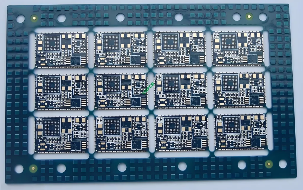
구조
4 층 다층 Bluetooth PCB의 구조는:
- 전도성 물질의 두 층: 절연층과 교대로 사용.
- 침지 금 표면 처리: 향상된 연결성 및 보호를 위해.
- 하프 홀 디자인: 특정 부품 배치 및 납땜 요구 사항.
특징
4 층 다층 Bluetooth PCB의 주요 기능에는 포함됩니다:
- 고급 레이어 구성: 4-우수한 신호 라우팅을위한 레이어 설계.
- 높은 정밀도: 4mil의 최소 트레이스 및 공간 크기 (0.1mm).
- 사용자 정의 가능한 색상 옵션: 흑백으로 제공됩니다.
- 표준두께: 완성두께 1.0mm로.
생산 과정
4 층 다층 Bluetooth PCB의 생산 프로세스에는 여러 단계가 포함됩니다.:
- 재료 준비: FR4 시트 및 동박 선택 및 준비.
- 레이어 스태킹: 구리와 절연 층을 결합합니다.
- 에칭: 원하는 회로 패턴을 형성하기 위해 여분의 구리를 제거합니다..
- 도금: 침지금 표면 처리 적용.
- 라미네이션: 열과 압력 하에서 층 결합.
- 교련: 관통 구멍 구성요소 및 비아용 구멍 생성.
- 솔더 마스크 적용: 솔더 브리지 및 환경 요인으로부터 회로 보호.
- 실크스크린 인쇄: 구성 요소 배치 및 식별을 위한 텍스트 및 기호 추가.
- 품질 관리: PCB가 모든 설계 사양 및 표준을 충족하는지 확인.
시나리오 사용
4 층 다층 Bluetooth PCB는 시나리오에 이상적입니다.:
- 높은 신호 무결성이 중요합니다.
- 안정적이고 내구성 있는 연결이 필요합니다..
- 안정적인 작동 온도를 유지하려면 효과적인 열 관리가 필요합니다..
- 성능 향상을 위해서는 고급 표면 처리가 필요합니다..


