
RO4350B Ceramic Hybrid High Frequency PCB Overview
The RO4350B Ceramic Hybrid High Frequency PCB is a cutting-edge printed circuit board designed for high-performance applications in the communication industry. Combining the robustness of Rogers RO4350B material with the versatility of FR4, this PCB offers exceptional electrical and thermal properties, making it ideal for high-frequency circuits.
재료 구성
The RO4350B Ceramic Hybrid High Frequency PCB is crafted from a unique blend of Rogers RO4350B and FR4 materials, pressed together to create a robust and reliable substrate. This mix ensures a balance of electrical performance and cost-effectiveness, 광범위한 응용 프로그램에 적합합니다.
성능 특성
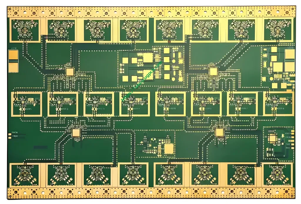
- 레이어 수: The PCB features an 8-layer design, providing ample space for complex circuitry and components.
- 유전 상수 (D k): With a D K of 3.48, the board exhibits stable electrical performance across a wide frequency range.
- 완성된 두께: The PCB has a finished thickness of 2.5mm, ensuring durability and structural integrity.
- 구리 두께: The 1oz copper thickness offers excellent conductivity and current carrying capacity.
- 유전체 두께: The dielectric layer is 0.338mm thick, contributing to the board’s overall electrical performance.
- 열전도율: With a thermal conductivity of 0.69w/m.k, the PCB effectively manages heat dissipation, preventing overheating and component failure.
- 가연성: The board meets the 94V-0 가연성 등급, ensuring safety in various environments.
생산 과정
The production of RO4350B Ceramic Hybrid High Frequency PCBs involves several precision steps:
- 재료 준비: Rogers RO4350B and FR4 materials are carefully selected and prepared for mixing.
- Mixing and Pressing: 재료는 제어 된 조건 하에서 혼합 및 함께 눌러 균일 한 기판을 형성합니다..
- 회로 설계 및 레이아웃: 원하는 회로 패턴은 고급 CAD 소프트웨어를 사용하여 설계 및 배치됩니다..
- 조작: PCB는 에칭을 포함한 일련의 프로세스를 통해 제조됩니다., 교련, 그리고 구리 도금.
- 표면 처리: 이사회는 전도도 및 부식 저항을 향상시키기 위해 침수 금 표면 처리를 거칩니다..
- 품질 관리: 각 PCB는 지정된 성능 표준을 충족하도록 엄격한 테스트를 거칩니다..
응용 시나리오
RO4350B 세라믹 하이브리드 고주파 PCB는 통신 기기에 사용하기에 이상적입니다., 포함:
- 고주파 회로: PCB의 뛰어난 전기 특성은 무선 및 전자 레인지 시스템의 고주파 회로에 적합합니다..
- 안테나 어레이: 강력한 설계 및 안정적인 성능은 통신 네트워크에서 복잡한 안테나 어레이의 작동을 지원합니다..
- 신호 처리 장치: PCB의 고속 신호를 처리하는 능력은 신호 처리 장치에서 신뢰할 수있는 성능을 보장합니다..
요약하면, RO4350B 세라믹 하이브리드 고주파 PCB는 통신 기기를위한 다목적 및 고성능 솔루션입니다., 전기 우수성의 조합을 제공합니다, 열 관리, 그리고 내구성.


