
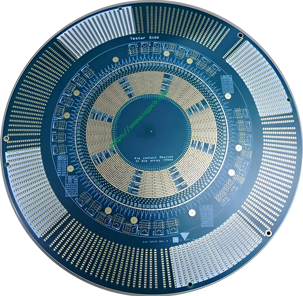
ATE Test Chip PCB Overview
The ATE test chip PCB is a specialized printed circuit board designed for use in automated test equipment (먹었다) systems for testing semiconductor chips. This PCB plays a crucial role in ensuring the quality and reliability of chips before they are integrated into electronic devices. Below is a detailed introduction to the ATE test chip PCB, 일반 정보를 다루고 있습니다, 분류, 재료, 성능, 구조, 특징, 생산 과정, 및 응용 프로그램 시나리오.
분류
ATE test chip PCBs are classified based on their layer count, 재료 구성, 및 특정 응용 프로그램 요구 사항. 여기에 소개 된 모델, ATE test chip PCB, is a 12-layer PCB, indicating its complexity and ability to handle intricate testing scenarios.
재료 구성
The ATE test chip PCB is constructed using isola 370hr material, a high-performance, high-reliability substrate known for its excellent electrical and thermal properties. This material ensures the PCB’s ability to withstand the demanding test conditions and provide stable performance.
성능 특성
The ATE test chip PCB excels in several performance areas, 고전류 운반 능력을 포함합니다, 낮은 신호 손실, 우수한 열 관리. The use of 2OZ copper thickness for inner layers and 1OZ for outer layers enhances its electrical conductivity and thermal dissipation capabilities. 추가적으로, the immersion gold (5유) surface finish provides superior corrosion resistance and solderability, ensuring reliable connections during testing.
구조 설계
구조적으로, the ATE test chip PCB features a board thickness of 3.0mm, 복잡한 회로 및 구성 요소를위한 강력한 기초 제공. The green color not only adds a visual distinction but also aids in inspection and troubleshooting processes.
독특한 특징
The ATE test chip PCB stands out with its unique features, including its high layer count, advanced material composition, and immersion gold surface finish. 이러한 기능, combined with its precise design and manufacturing processes, make it an ideal choice for ATE chip testing applications.
생산 과정
The production of ATE test chip PCBs involves a series of sophisticated steps:
- 재료 준비: The isola 370hr substrate is prepared and cut to the required dimensions.
- 구리 라미네이션: 구리 호일은 기판에 적층된다, with specific attention to the inner layer 2OZ and outer layer 1OZ thickness requirements.
- 회로 패터닝: 원하는 회로 패턴은 정밀 에칭 기술을 사용하여 구리 포일에 에칭됩니다..
- 층 스태킹 및 라미네이션: 다중 층이 쌓여 함께 적층됩니다, 정확한 정렬 및 결합 보장.
- 시추 및 도금: 구성 요소 장착 및 상호 연결을 위해 구멍이 뚫린다, and then plated to enhance conductivity.
- 표면 마감 적용: The immersion gold (5유) coating is applied to provide corrosion resistance and solderability.
- 최종 검사 및 테스트: PCB는 사양 및 성능 요구 사항을 준수하기 위해 엄격한 검사 및 테스트를 거칩니다..
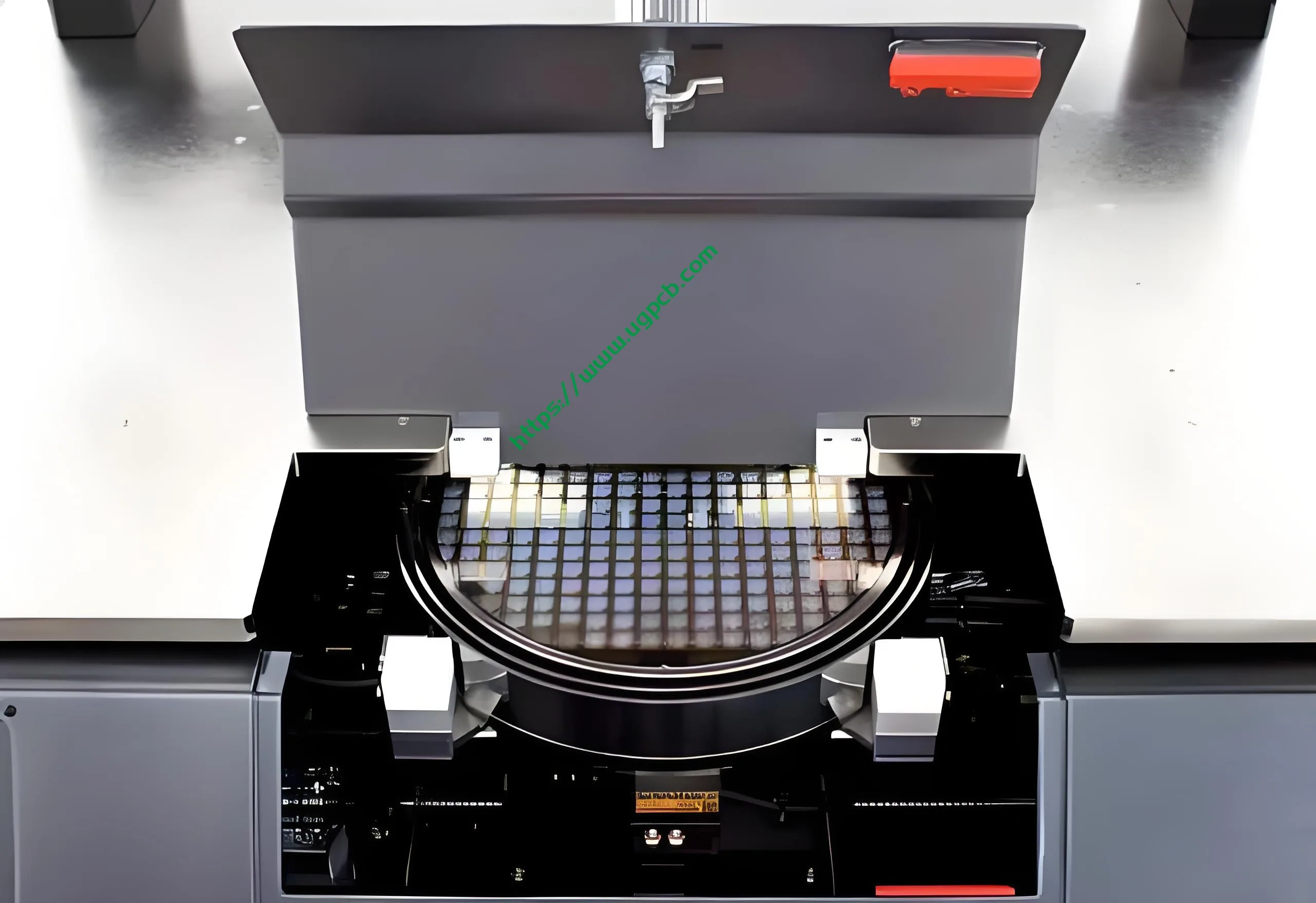
응용 시나리오
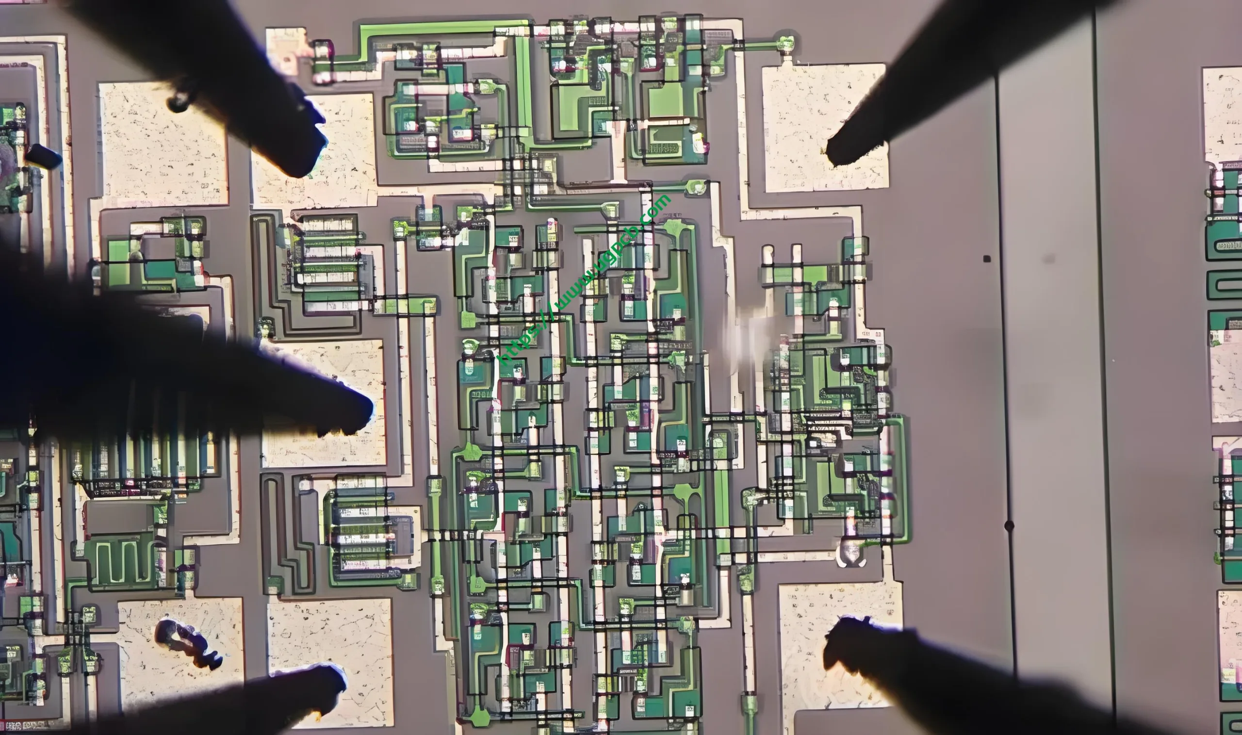
ATE test chip PCBs are primarily used in automated test equipment systems for the testing and validation of semiconductor chips. 그것들은 반도체 산업에서 필수적입니다, where high-reliability testing is crucial for ensuring the quality and performance of chips before they are integrated into electronic devices. By utilizing ATE test chip PCBs, manufacturers can quickly and accurately identify any defects or issues in the chips, ensuring that only high-quality products are shipped to customers.


