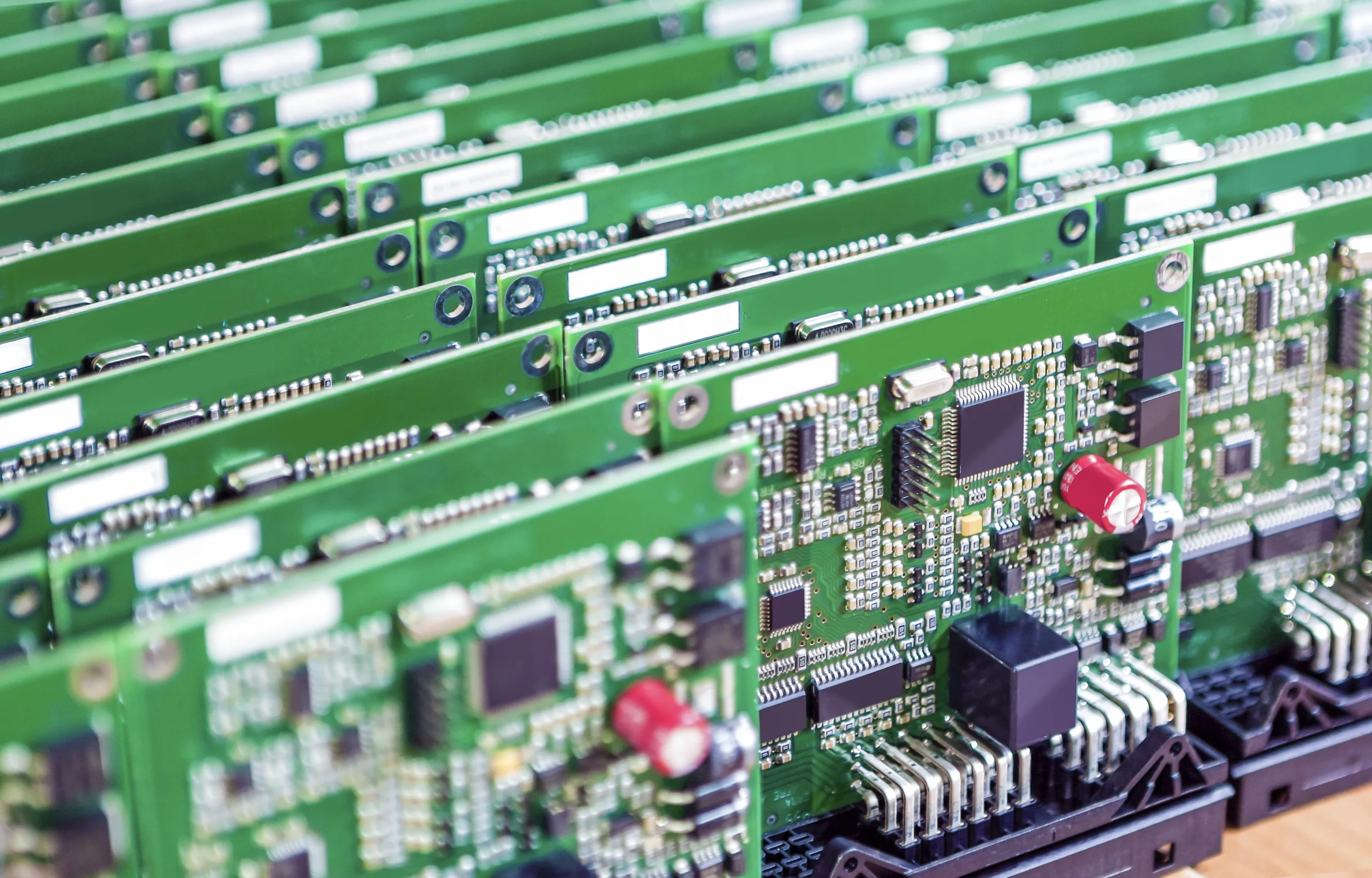
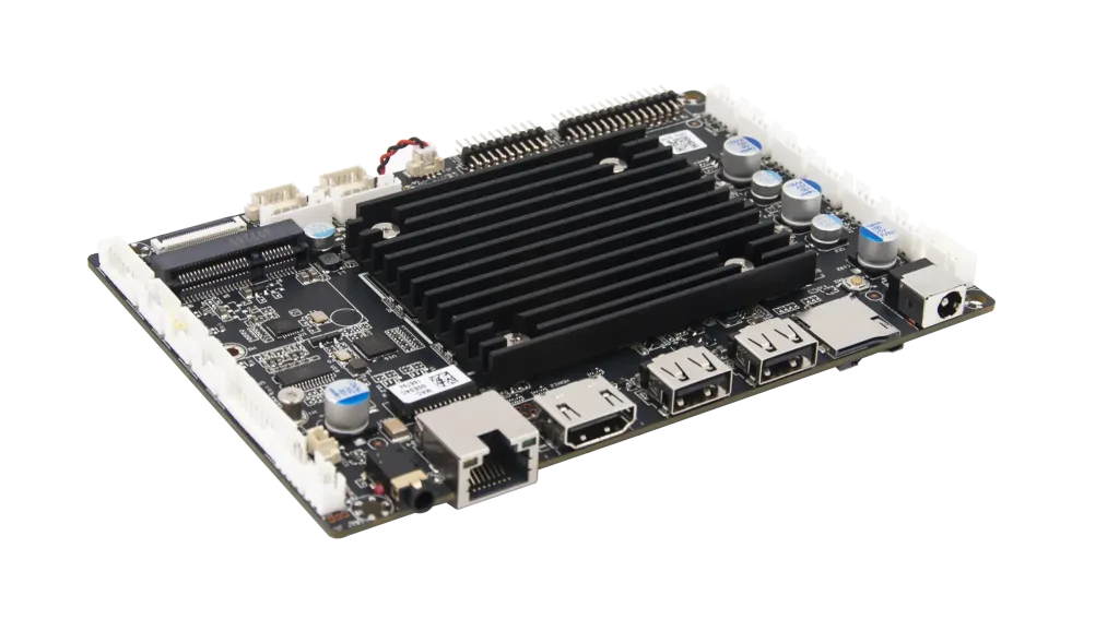
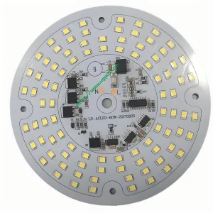
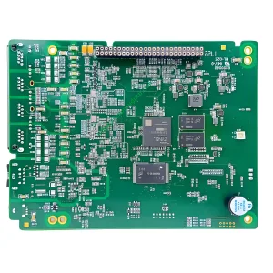
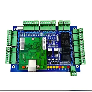
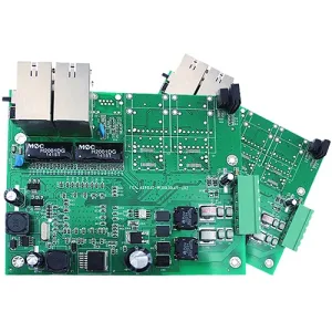
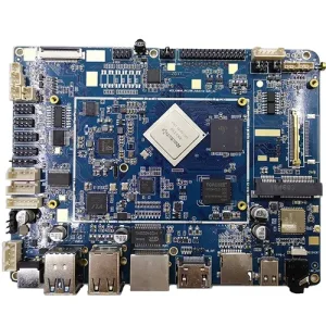
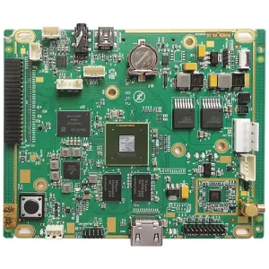
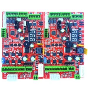
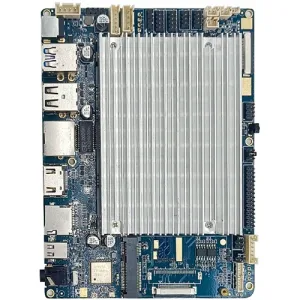
In the PCB assembly industry, DIP stands for Dual In-line Package. It refers to a type of electronic component package with a rectangular housing and two parallel rows of electrical connection pins. The pins are all parallel, pointing downwards, and extend beyond the bottom plane of the package, long enough to be inserted through holes in the printed circuit board (PCB) and soldered on the other side.
DIP is not the same as SMT (표면 실장 기술). SMT is a popular technology and process in the electronic assembly industry that involves mounting surface-mount components on the surface of a circuit board or other substrate and assembling them by reflow soldering or dip soldering.
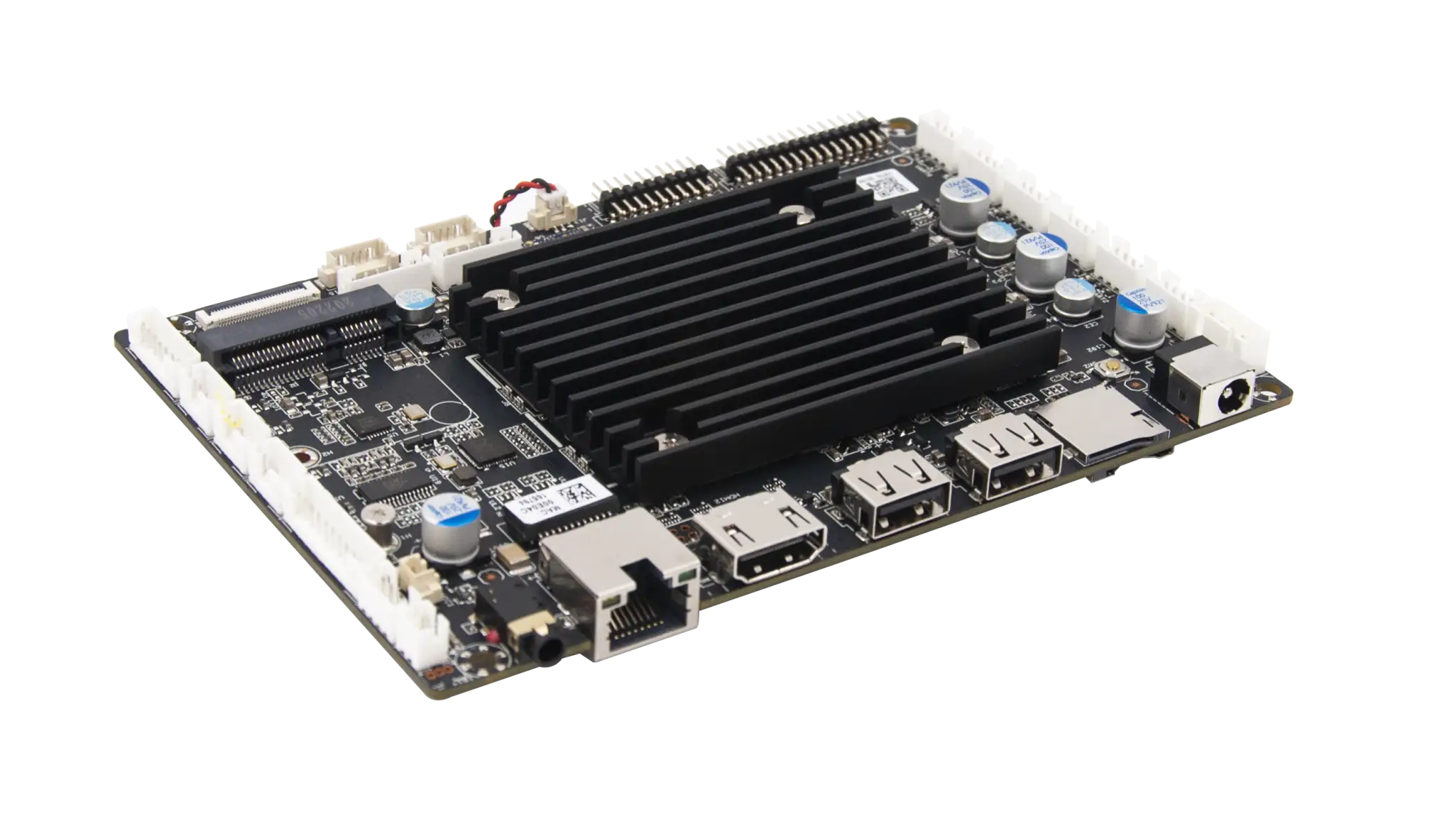
The difference between SMT and DIP lies in the installation method. SMT is usually installed on the surface of components without leads or with short leads. It requires printing solder paste on the circuit board first, then placing it through a pick-and-place machine, and finally fixing the components by reflow soldering. 담그다, 반면에, is a through-hole packaging device that is fixed by wave soldering or manual soldering.
Both SMT and DIP are part of PCBA processing, but not all PCBA factories have the capability for both SMT and post-DIP soldering, and the quality of processing varies. When choosing a cooperative PCBA factory, it is recommended to visit the factory in person to observe the technical expertise of the staff, processing equipment, and overall environment.
PCB assembly requires knowledge beyond just PCB components and assembly; it also necessitates expertise in printed circuit board design, 공들여 나열한 것, PCB 제조, and final product application. AuSPI offers a one-stop solution for all circuit board production services—manufacturing, testing/inspection, 그리고 조립. Our clients hire us as their full or partial turnkey supplier from manufacturing to assembly and testing. Through our strong network of proven partners, we can provide the most advanced and virtually unlimited capabilities for your prototype or production PCB run.
 UGPCB 로고
