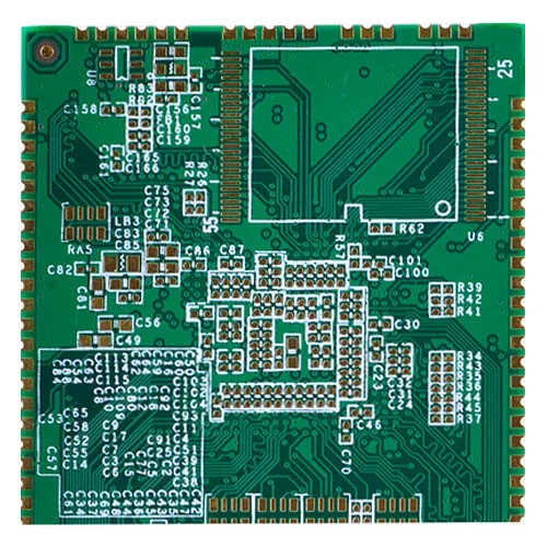
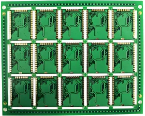
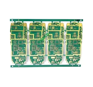
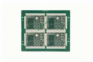
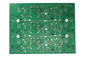
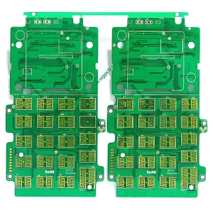
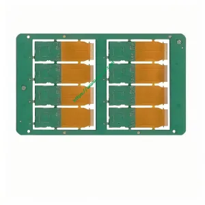
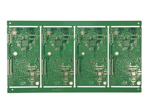
Introduction to HDI Mouse Bite PCB
HDI (고밀도 상호 연결) technology is a significant advancement in the field of printed circuit boards (PCB), allowing for more complex and compact electronic designs. The HDI Mouse Bite PCB, specifically, is a high-density interconnect board designed with precision and efficiency in mind. This type of PCB is ideal for applications demanding high signal integrity, smaller form factors, and greater performance.
정의 및 설계 요구 사항
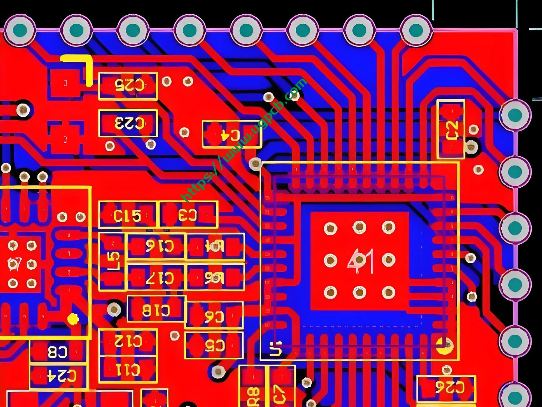
An HDI Mouse Bite PCB refers to a multilayer PCB that incorporates advanced fabrication techniques to achieve higher wiring density and finer features than standard PCBs. 용어 “mouse bite” describes the unique shape of the inner layers, which are staggered or “bitten” into to allow for more efficient space utilization. The design requirements for an HDI Mouse Bite PCB include precise layer stacking, tight tolerances, and specialized materials to ensure optimal performance and reliability.
작동 원리
The working principle behind an HDI Mouse Bite PCB involves creating multiple layers of conductive material, separated by insulating layers, with intricate patterns etched onto each layer. These layers are then aligned and bonded together using heat and pressure. The unique “mouse bite” configuration allows for increased routing density by staggering the layers, reducing the need for vias and enhancing signal integrity.
응용 및 분류
HDI Mouse Bite PCBs are primarily used in consumer electronics where space is at a premium, and performance is paramount. They are commonly found in smartphones, 정제, 웨어러블 기기, and other portable electronics. Based on their complexity and the number of layers, HDI PCBs can be classified into different categories, such as Type I, Type II, and Type III, each offering varying levels of density and functionality.
재료 및 성능
The HDI Mouse Bite PCB is constructed using high-quality materials like SY S1000-2, which provides excellent electrical properties and thermal stability. The finished thickness of 0.8mm ensures durability without compromising on the slim profile required for modern electronics. With a copper thickness of 1OZ/1OZ, these PCBs offer robust conductivity. The surface treatment, 동의하다 (무전해 니켈 침지 금), enhances solderability and corrosion resistance, ensuring long-term performance.
구조와 특징
The structure of an HDI Mouse Bite PCB includes multiple layers of conductive copper, precision-etched with fine traces and spaces as small as 3mil/3mil. The unique staggered layering, 또는 “mouse bite,” allows for increased routing density and improved signal integrity. Key features include high thermal conductivity, 낮은 유전 상수, and superior mechanical strength, making them suitable for high-performance applications.
생산 과정
The production process of an HDI Mouse Bite PCB involves several sophisticated steps, 포함:
- 재료 준비: Selecting high-quality substrate materials and copper foils.
- 레이어 스태킹: Arranging the layers in a specific order to achieve the desired “mouse bite” effect.
- 본딩: 열과 압력을 사용하여 층을 서로 결합, forming a single, cohesive unit.
- 에칭: 과잉 구리를 제거하기 위해 식각액 적용, 원하는 전도성 경로만 남기고.
- 도금: Adding a thin layer of metal to the exposed copper to improve conductivity and solderability.
- 표면 처리: Applying ENIG to protect against oxidation and enhance solderability.
- 품질 관리: 각 보드가 엄격한 품질 표준을 충족하는지 확인하기 위해 철저한 검사와 테스트를 수행합니다..
사용 사례 및 시나리오
HDI Mouse Bite PCBs are ideal for use in consumer electronics where miniaturization and high performance are critical. 일반적인 응용 프로그램은 다음과 같습니다:
- 스마트폰: 기능이나 성능 저하 없이 더욱 슬림한 디자인 구현.
- 정제: 고속 데이터 전송 및 처리를 위한 안정적인 연결 제공.
- 웨어러블 기기: 견고한 성능과 내구성을 유지하면서 컴팩트한 디자인을 지원합니다..
- Portable Media Players: Ensuring high-quality audio and video processing capabilities in a small form factor.
결론적으로, the HDI Mouse Bite PCB represents a pinnacle of innovation in PCB technology, offering unmatched density, 성능, and reliability for the most demanding consumer electronic applications.
 UGPCB 로고

