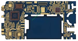
Introduction to Type-C Connector PCB
The Type-C Connector PCB is an advanced electronic component designed for high-speed data and power transmission. This guide provides a comprehensive overview of the product, including its definition, 디자인 요구 사항, 작동 원리, uses, 분류, 재료, 성능, 구조, 특징, manufacturing process, and typical application scenarios.
정의
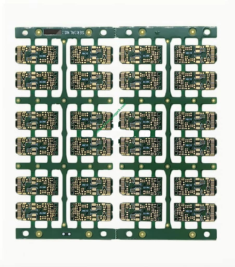
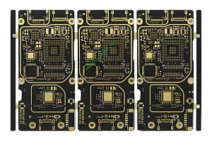
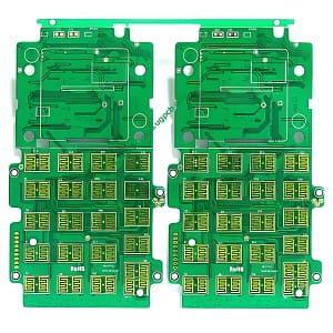
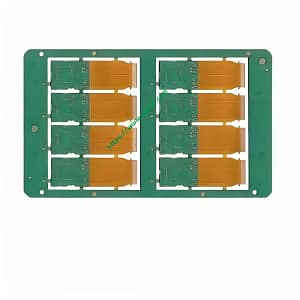
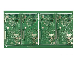
A Type-C Connector PCB (인쇄 회로 기판) 전문이다 회로 기판 that incorporates a USB Type-C connector. It is designed to support high-speed data transfer and power delivery, making it ideal for modern electronic devices.
설계 요구 사항
The design of a Type-C Connector PCB must adhere to specific standards to ensure optimal performance and reliability. Key design requirements include:
High-Speed Data Transmission
Supports USB 3.1 Gen 2 or higher standards for fast data transfer rates.
Power Delivery
Capable of handling up to 100W of power delivery, suitable for charging and powering devices.
최소한의 추적/공간
Ensures fine pitch components can be placed accurately with a minimum trace/space of 3mil/3mil.
Precision Tolerances
Maintains strict tolerance requirements for outline and PSR (Pick and Place Reliability).

작동 원리
The Type-C Connector PCB operates based on the principles of electrical conductivity and signal integrity. It utilizes copper traces embedded in a high TG FR4 substrate to transmit signals between the Type-C connector and other electronic components on the board. The immersion gold and OSP surface treatments enhance conductivity and protect against oxidation.
용도
Type-C Connector PCBs are used in a variety of applications where high-speed data transfer and power delivery are essential. Common uses include:
Data Transfer
Facilitates quick and efficient data transfer between devices such as laptops, 스마트폰, and external storage devices.
전원공급장치
Provides reliable power delivery for charging batteries and powering electronic devices.
Device Connectivity
Enables connectivity between various devices, enhancing the functionality and versatility of electronic systems.
Classifications
Type-C Connector PCBs can be classified based on several criteria:
레이어 수에 의해
다층 PCB, such as the 6-layer HDI (고밀도 상호 연결) PCB mentioned.
재료로
Constructed from high TG FR4 material for enhanced thermal stability.
표면 처리에 의한
Features immersion gold and OSP (유기 용해성 보존) surface treatments for improved conductivity and durability.
재료
The primary materials used in the construction of Type-C Connector PCBs include:
높은 TG FR4
A flame-retardant glass-reinforced epoxy laminate material known for its high thermal stability and mechanical strength.
구리
Used for the conductive traces, with a standard thickness of 1OZ.
Green/White Color (PSR: TAIYO INK)
The color of the PCB, achieved using TAIYO INK for consistent and vibrant results.
성능
The performance of Type-C Connector PCBs is characterized by:
높은 신호 무결성
Ensures minimal loss of signal quality over long distances and high frequencies.
내구성
Resistant to environmental factors such as temperature variations and humidity.
신뢰할 수 있음
Designed to withstand repeated connections and disconnections without degradation.
구조
The structure of a Type-C Connector PCB typically includes:
Multi-Layer Design
A 6-layer HDI PCB with 2+N+2 layer configuration for complex circuitry.
Fine Pitch Components
Allows for the integration of fine pitch components with a minimum hole size of 0.2mm for mechanical holes and 0.1mm for laser holes.
Advanced Surface Treatments
Immersion gold and OSP coatings enhance conductivity and protect against corrosion.
특징
Key features of Type-C Connector PCBs include:
High-Speed Data and Power Transmission
Supports USB 3.1 Gen 2 or higher standards for rapid data transfer and up to 100W power delivery.
소형 디자인
Slim profile with a finished thickness of 0.8mm, suitable for slim and sleek device designs.
강력한 건축
Made from high TG FR4 material for enhanced durability and thermal stability.
생산 과정
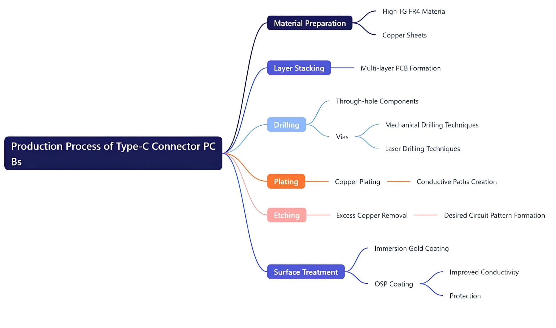
The production of Type-C Connector PCBs involves several steps:
재료 준비
Selection of high TG FR4 material and copper sheets.
레이어 스태킹
Stacking of multiple layers to form a multi-layer PCB.
교련
Creation of holes for through-hole components and vias using mechanical and laser drilling techniques.
도금
Application of copper plating to create conductive paths.
에칭
Removal of excess copper to form the desired circuit pattern.
표면 처리
Application of immersion gold and OSP coatings for improved conductivity and protection.
일반적인 응용 프로그램 시나리오
Type-C Connector PCBs are widely used in various applications, 포함:
가전제품
스마트폰, 정제, 노트북, 및 기타 휴대용 장치.

자동차 산업
In-car entertainment systems and charging solutions.
산업용 장비
Control panels and communication devices requiring robust connectivity.
By understanding these aspects, you can appreciate the versatility and importance of Type-C Connector PCBs in modern electronic design.
 UGPCB 로고

