
Introduction to IC Chip Test PCB
개요 및 정의
An IC Chip Test PCB, or Integrated Circuit Chip Test Printed Circuit Board, is a specialized circuit board designed for testing integrated circuit chips. It ensures that the chips meet the required specifications before they are used in electronic devices.
작동 원리
The IC Chip Test PCB works by connecting the integrated circuit chip to various test points on the PCB. These test points measure the electrical characteristics of the chip, such as voltage, 현재의, 그리고 저항, to verify its functionality.
응용
IC Chip Test PCBs are used in the manufacturing and quality control processes of electronic devices. They are essential for ensuring that only functioning and reliable chips are used in the final products.
Types of IC Chip Test PCBs
There are different types of IC Chip Test PCBs based on their design and functionality:
- Functional Test PCBs: Used to test the overall functionality of the chip.
- Parameter Test PCBs: Used to measure specific parameters like power consumption, 속도, 그리고 온도.
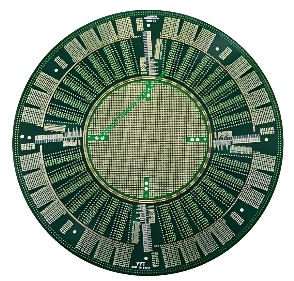
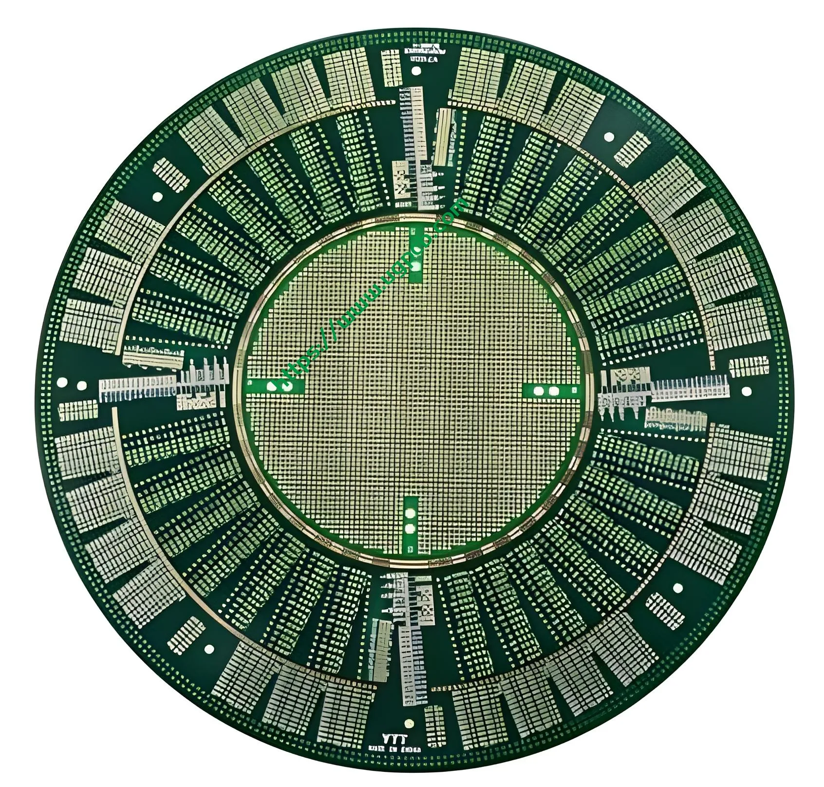
재료 및 건축
- 재료: TU872SLS, a high-quality epoxy material.
- 레이어: 20 레이어, providing robustness and better signal integrity.
- 색상: 녹색 또는 흰색으로 제공됩니다..
- 완성된 두께: 2.0mm, ensuring durability while being slim.
- 구리 두께: 1온스, which offers good conductivity.
- 표면 처리: Immersion gold with a thickness of at least 3U”, enhancing corrosion resistance and solderability.
성능 특성
IC Chip Test PCBs are designed to accurately test the performance of integrated circuit chips. They support high-speed data transfer and are built to withstand repeated usage over time. The immersion gold finish ensures long-lasting performance and reliability.
구조적 특징
The structure of an IC Chip Test PCB includes multiple layers of copper traces sandwiched between layers of substrate material. This multilayer design helps in managing heat dissipation and improving electrical performance. The PCB is coated with a protective layer to prevent damage and ensure longevity.
생산 과정
The production of an IC Chip Test PCB involves several steps:
- 설계: Using specialized software to create the circuit layout.
- 에칭: Removing excess copper to form the desired patterns.
- 라미네이션: Combining multiple layers together.
- 도금: Adding a thin layer of metal to improve connectivity.
- 점검: Ensuring the PCB meets quality standards.
- 집회: Mounting components onto the PCB.
- 테스트: Verifying functionality and performance.
사용 사례
IC Chip Test PCBs are used in various applications including:
- 가전제품: 휴대 전화, 정제, smartwatches.
- 자동차: In-car systems for navigation and entertainment.
- 의료 기기: Portable medical equipment.
- 산업 자동화: Control systems for machinery and robotics.
결론적으로, IC Chip Test PCBs play a crucial role in the electronics manufacturing process by ensuring the reliability and functionality of integrated circuit chips. Their widespread adoption across different industries highlights their versatility and importance in modern electronic devices.


