Base Plate Structure and Positioning
고주파 하이브리드 부목에는베이스 플레이트가 포함됩니다, 첫 번째 내부 와이어 층에 접고 배치됩니다., 첫 번째 외부 와이어 레이어, and the top surface of the solder mask ink layer from bottom to top in order.
Layer Composition and Auxiliary Area Fixation
The second layer of solder resist ink layer is also present. 기판에는 고주파 면적과 보조 영역이 포함됩니다.. 보조 영역이 마침내 고정되어 있습니다, 고주파 지역의 인레이는 고정 위치에 있어야합니다..
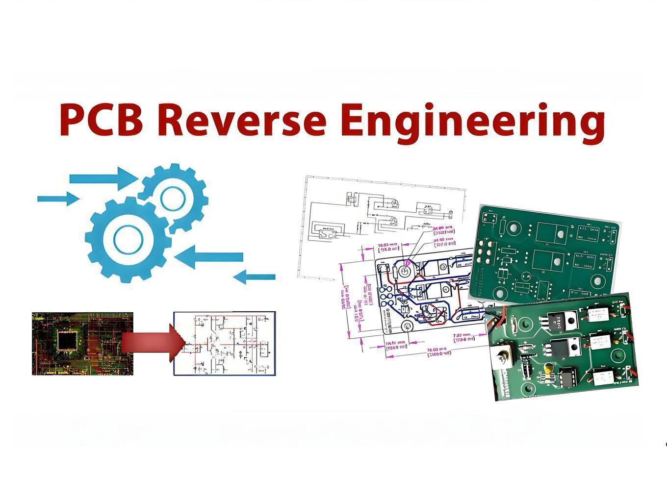
High-Frequency Hybrid Splint Utility Model
Division into High-Frequency and Auxiliary Areas
유틸리티 모델은 고주파 하이브리드 부목을 제공합니다, 두 부분으로 나뉩니다: 고주파 지역 및 보조 영역. These areas provide mechanical support.
Independent Arrangement of High-Frequency Area
유틸리티 모델은 고주파 영역이 독립적으로 배열되어 있음을 공개합니다.. Only the high-frequency area is made of high-frequency materials. This minimizes the use of high-frequency board materials and reduces production cost while satisfying high-frequency signals.
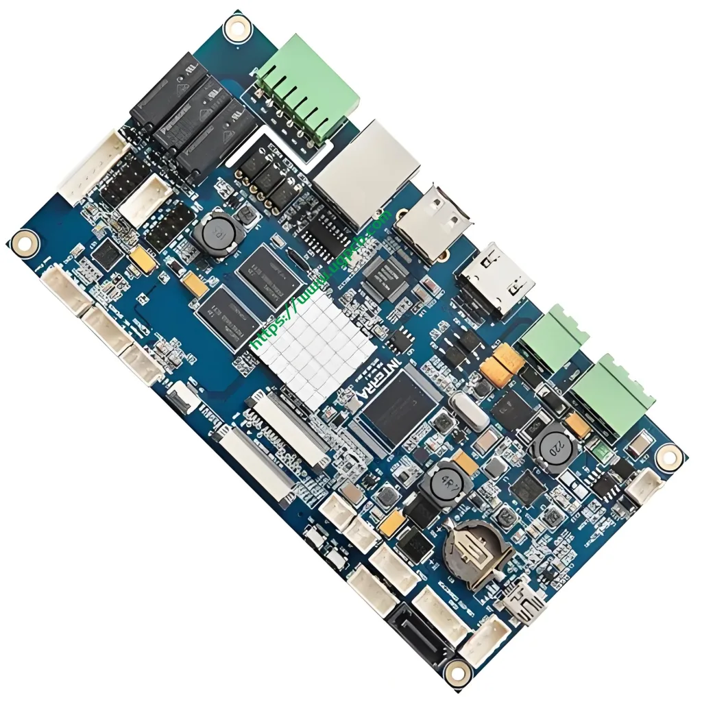
High Frequency Hybrid Product Specifications
Classification and Material
- 레이어: 6
- 중고 보드: RO4350B + FR4
- 두께: 1.6mm
- 크기: 210mm*280mm
Surface Treatment and Aperture
- 표면 처리: 금도금
- 최소 조리개: 0.25mm
Application and Features
- 애플리케이션: 의사소통
- 특징: 고주파 혼합 압력
By following these specifications and design principles, UGPCB (formerly known as kingford) ensures optimal performance and cost-effectiveness in high-frequency applications.


