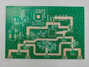
Overview of Microwave Hybrid PCB
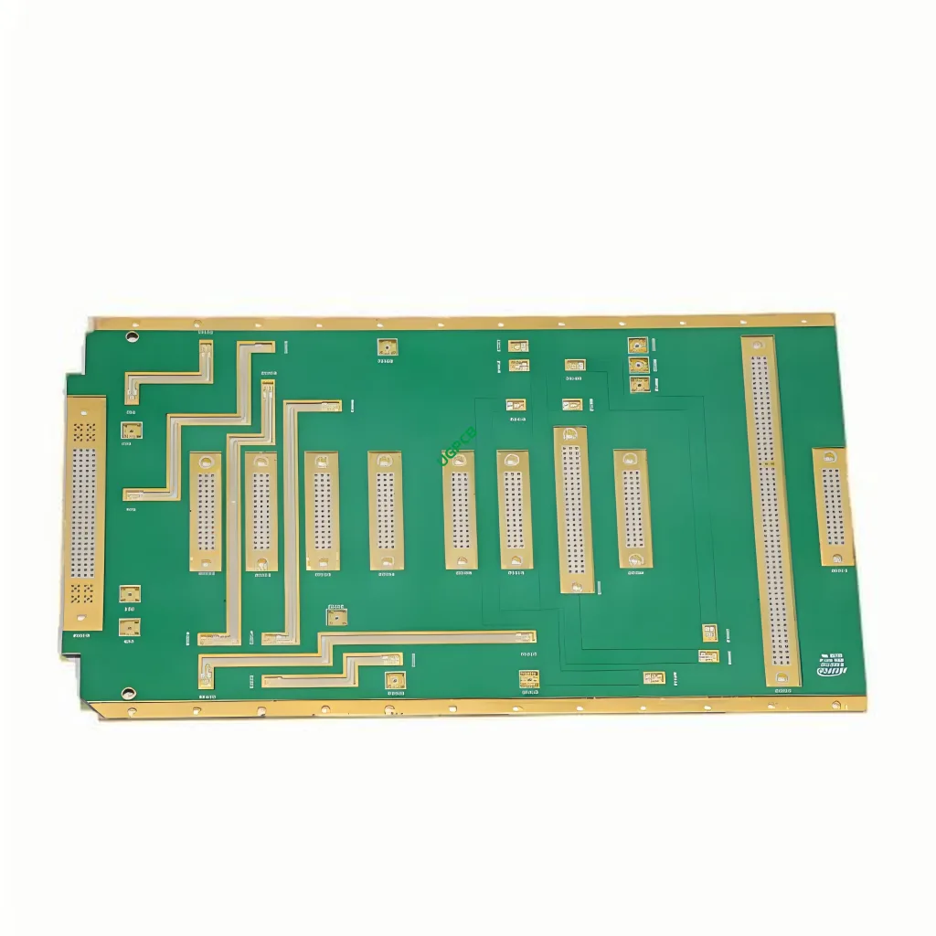
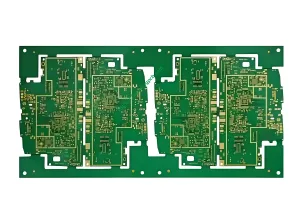
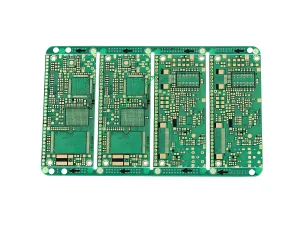
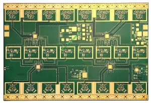
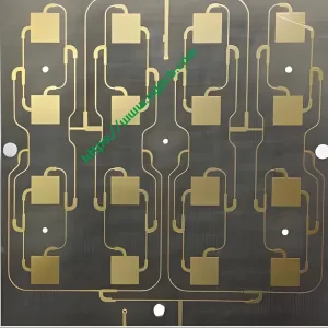
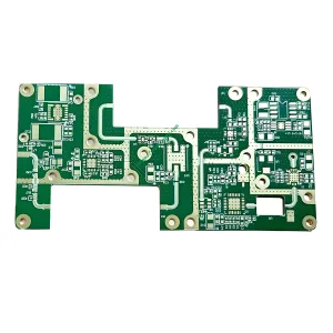
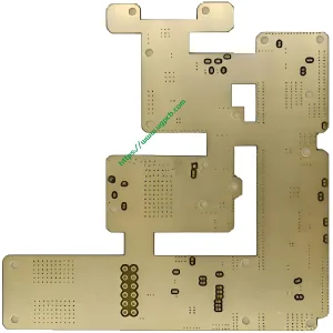
Microwave Hybrid PCB, also known as Hybrid Printed Circuit Board, is a specialized type of circuit board designed for high-frequency applications. It combines the benefits of traditional FR4 material and advanced materials like Teflon and ceramic to meet stringent performance requirements in various industries.
Definition and Design Considerations
A Hybrid PCB integrates different substrate materials within a single board. This design approach allows for optimizing dielectric constants (~에 이르기까지 2.2 에게 16) and tailoring the board’s properties for specific high-frequency needs. Key design considerations include material selection, layer stack-up, and impedance control to ensure signal integrity and minimize losses.
작업 원칙 및 응용 프로그램
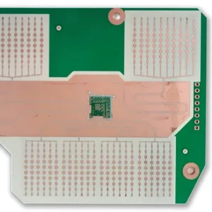
The working principle revolves around managing electromagnetic waves at microwave frequencies efficiently. By using a combination of low and high dielectric constant materials, Hybrid PCBs can achieve better impedance matching, reduced signal loss, and enhanced overall performance. They are widely used in telecommunications, 레이더 시스템, 위성 통신, and other high-frequency microwave applications.
분류 및 재료
유형:
- 2-Layer to Multi-Layer Hybrid PCBs: Depending on complexity, these boards can range from two layers up to multiple layers, accommodating intricate circuit designs.
- Thickness Variants: Available in thicknesses from 0.1mm to 12mm, providing flexibility for different application requirements.
Core Materials:
- 테프론: Known for its low dielectric constant and loss tangent, 고주파 응용 프로그램에 이상적입니다.
- 세라믹 + FR4: Combines the thermal stability of ceramic with the mechanical robustness of FR4, offering a balanced solution for many designs.
성능 및 구조
Hybrid PCBs excel in high-frequency performance due to their carefully selected materials and precise manufacturing processes. They feature controlled copper thickness (from 0.5oz to 3oz), which directly impacts current-carrying capacity and heat dissipation. The surface technology options, including Silver, 금, 그리고 OSP (유기 납땜성 방부제), further enhance solderability and corrosion resistance.
Characteristics and Production Process
Key characteristics of Microwave Hybrid PCBs include:
- Enhanced signal integrity through optimized dielectric constants.
- 우수한 열 관리 기능.
- Customizable to meet specific application needs regarding frequency range, power handling, and environmental conditions.
생산 과정에는 여러 단계가 포함됩니다.:
- 재료 선택: Choosing appropriate core and prepreg materials based on design specifications.
- 라미네이션: Combining layers under pressure and heat to form a solid board structure.
- 에칭: Removing unwanted copper to create the desired circuit pattern.
- 표면 마무리: Applying the chosen surface treatment to protect against oxidation and improve solderability.
- 품질 보증: Ensuring the final product meets IPC6012 Class 2 또는 3 표준, guaranteeing reliability and performance.
시나리오 사용
Microwave Hybrid PCBs are essential in scenarios where conventional PCBs cannot provide the necessary performance levels. These include but are not limited to:
- 통신 인프라, such as base stations and antennas.
- Aerospace and defense systems requiring reliable high-frequency operation.
- Medical equipment utilizing microwave technology for diagnostics or treatment.
- High-speed data communication networks and servers.
요약하면, Microwave Hybrid PCBs represent a sophisticated solution for demanding high-frequency applications, combining advanced materials and precise engineering to deliver exceptional performance and reliability.
 UGPCB 로고

