Reduction of Assembly Errors
Precise Design and Automated Production
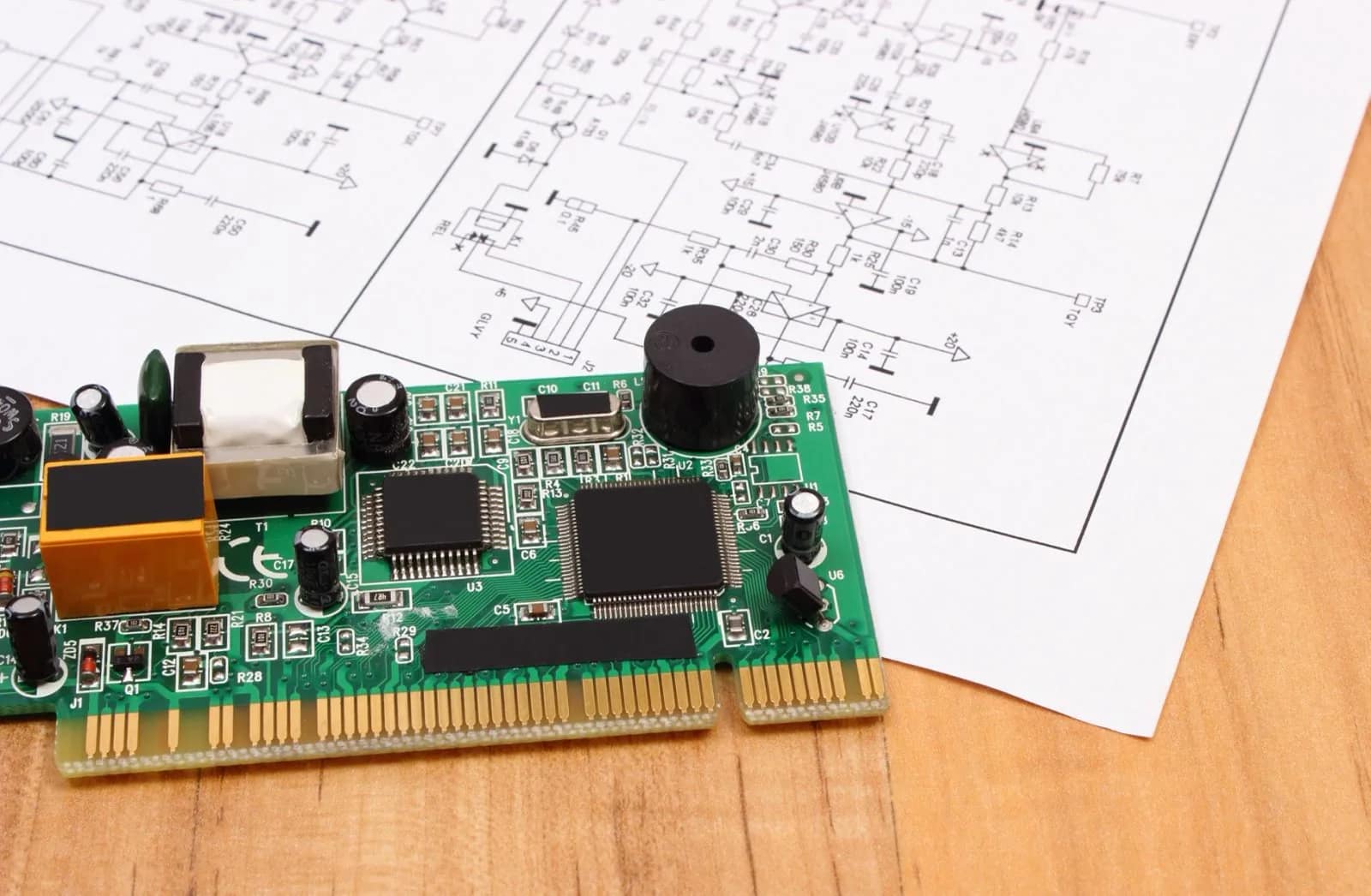
유연한 인쇄 회로에는 많은 이점이 있습니다, 포함:
- Reduce Assembly Errors: Through precise design and automated production, flex circuits eliminate human error in manual wiring harnesses. Except for errors caused by production, circuits are routed only to those points required by the exact design plan.
Cost and Time Efficiency
Reduced Assembly Time and Cost
- 조립 시간과 비용 절감: 플렉스 회로는 조립 중에 노동력이 적고 생산 오류를 줄입니다.. 유연한 회로는 형태를 통합하는 고유의 능력을 가지고 있습니다, fit, and function. 플렉스 회로는 높은 라우팅 비용을 제거합니다, wrapping, and soldering wires. Install or replace a complete interconnect system instead of individual hard PC boards. 결과적으로, wiring errors are eliminated, thereby reducing manufacturing costs. 조립 시간과 비용을 줄일 수 있습니다, 복잡한 회로의 저성 생산 또는 간단한 회로의 대량 생산에 관계없이.
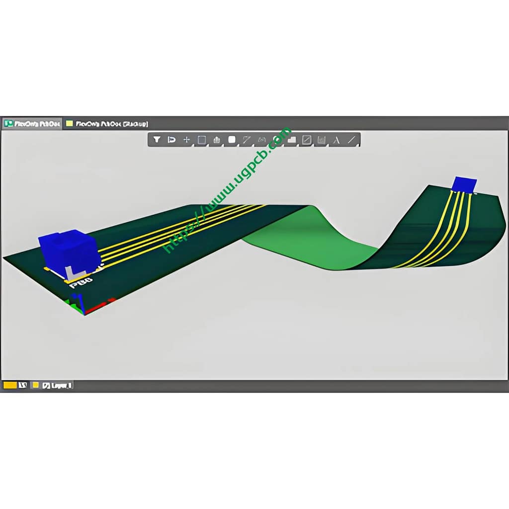
Design Freedom
Endless Design Options
- 디자인 자유: Unlike rigid circuit boards, 플렉스 회로는 2 차원으로 제한되지 않습니다. 와이어 또는 리본 케이블만큼 유연하기 때문에, the flex circuit design options are endless. UGPCB에, we pride ourselves on being able to tackle the most complex design challenges. Flexible circuits can be designed to meet highly complex and unimaginable configurations, while being able to operate in the harshest environments.


