
Plugged with Epoxy Resin Multilayer PCB: 포괄적 인 개요
제품 프로필
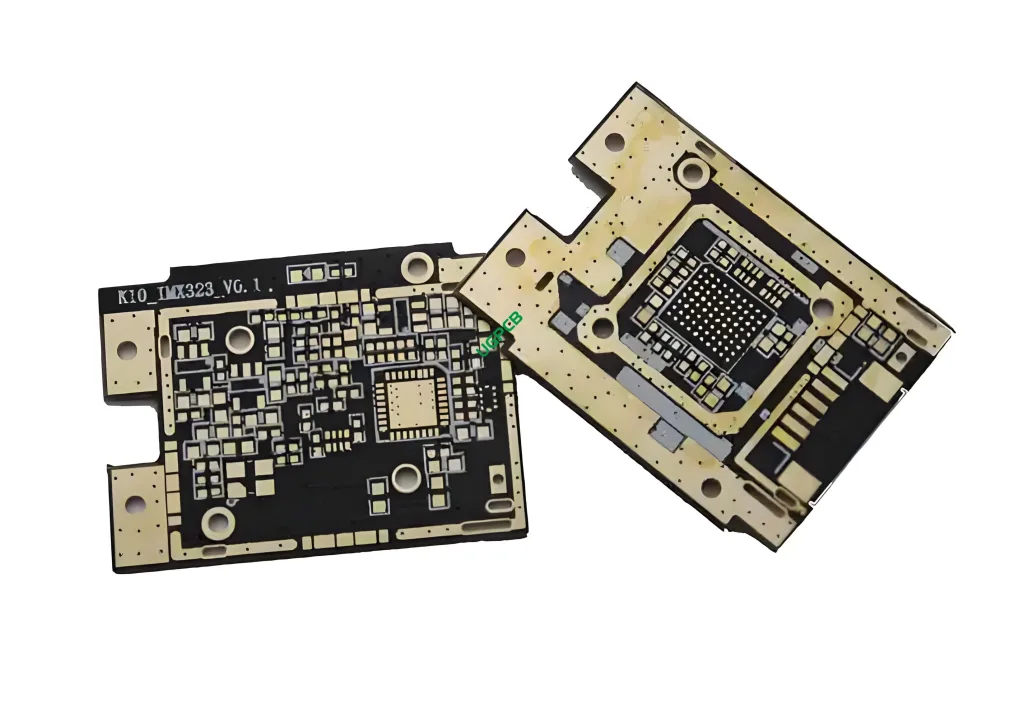
The Plugged with Epoxy Resin Multilayer PCB is a high-performance electronic component designed for complex circuitry applications. This PCB stands out due to its use of epoxy resin plugging, which enhances its durability and reliability.
정의
A Plugged with Epoxy Resin Multilayer PCB refers to a printed circuit board (PCB) that features multiple layers of conductive and non-conductive materials, with epoxy resin used to fill through-holes. This technique ensures robust mechanical support and improved electrical performance.
설계 요구 사항
The design specifications of this PCB are meticulously crafted to meet high standards:
- 재료: Premium FR4, 우수한 열 및 전기 특성으로 유명합니다.
- 레이어: Eight layers, allowing for intricate circuit designs and compact form factors.
- 색상: Available in Green and White, offering aesthetic flexibility.
- 완성된 두께: 1.2mm, providing a balance between structural integrity and space efficiency.
- 구리 두께: 1온스, ensuring reliable electrical conductivity.
- 표면 처리: 이머젼 골드, 납땜 가능성 및 부식성 향상.
- 최소 추적/공간: 4밀(0.1mm), 미세한 디테일 및 고밀도 레이아웃을 허용합니다.
작동 원리
This PCB operates by facilitating the flow of electrical signals through its multilayer structure. The epoxy resin plugging helps in maintaining signal integrity by preventing short circuits and reducing electromagnetic interference (EMI).
응용
The Plugged with Epoxy Resin Multilayer PCB is widely used in:
- High-Performance Electronics: Such as advanced computing systems and telecommunications equipment.
- Automotive Industry: For engine control units and other critical systems.
- 항공우주 및 국방: Where reliability under extreme conditions is crucial.
- 의료 기기: Ensuring precision and reliability in diagnostic and therapeutic equipment.
유형 및 분류
This PCB can be classified based on several criteria:
- 기술 별: Combination of SMD and THD technologies.
- 응용 프로그램에 의해: General purpose or specific industries like automotive, 항공우주, and medical.
- 레이어 수에 의해: Eight layers, suitable for complex circuitry.
재료 구성
주로 FR4에서 구성됩니다, 이 PCB 자료는 제공됩니다:
- 우수한 열 안정성
- 높은 기계적 강도
- 우수한 전기 절연 특성
성능 지표
주요 성능 지표에는 포함됩니다:
- 신호 무결성: 신중한 레이아웃 설계 및 임피던스 매칭을 통해 유지됩니다.
- 신뢰할 수 있음: Ensured by rigorous testing protocols and quality control measures.
- 호환성: With a wide range of electronic components and systems.
구조적 특징
The PCB’s structure comprises:
- Multilayer stackup for enhanced signal integrity
- Precision-etched traces and spaces for fine circuitry
- Robust through-hole plating for durable mechanical connections
Distinctive Traits
Notable characteristics include:
- Versatility in mounting options (SMD and THD)
- High signal-to-noise ratio due to optimized layout
- 습도 및 온도 변화와 같은 환경 요인에 대한 저항
생산 워크 플로
제조 공정에는 여러 단계가 포함됩니다:
- 디자인 및 레이아웃: Using advanced CAD software to create precise schematics.
- 재료 준비: Cutting FR4 sheets to size and cleaning them thoroughly.
- 에칭: Applying etchant to remove unwanted copper from the board.
- 도금: 표면 마무리를 위해 금 욕조에 보드를 담그기.
- 집회: 납땜 표면 마운트 및 통로 구성 요소가 정확하게.
- 테스트: 사양 준수를 보장하기 위해 기능 테스트를 수행합니다.
- 품질 관리: 결함 및 성능 검증에 대한 최종 검사.
사용 사례
이 PCB가 응용 프로그램이 포함하는 일반적인 시나리오:
- Advanced Computing Systems
- Automotive Engine Control Units
- Aerospace Communication Systems
- Medical Diagnostic Equipment
요약하면, the Plugged with Epoxy Resin Multilayer PCB represents a cutting-edge solution for demanding electronic applications. Its unique combination of advanced materials, meticulous design, and robust manufacturing processes ensures unparalleled performance and reliability across various industries.


