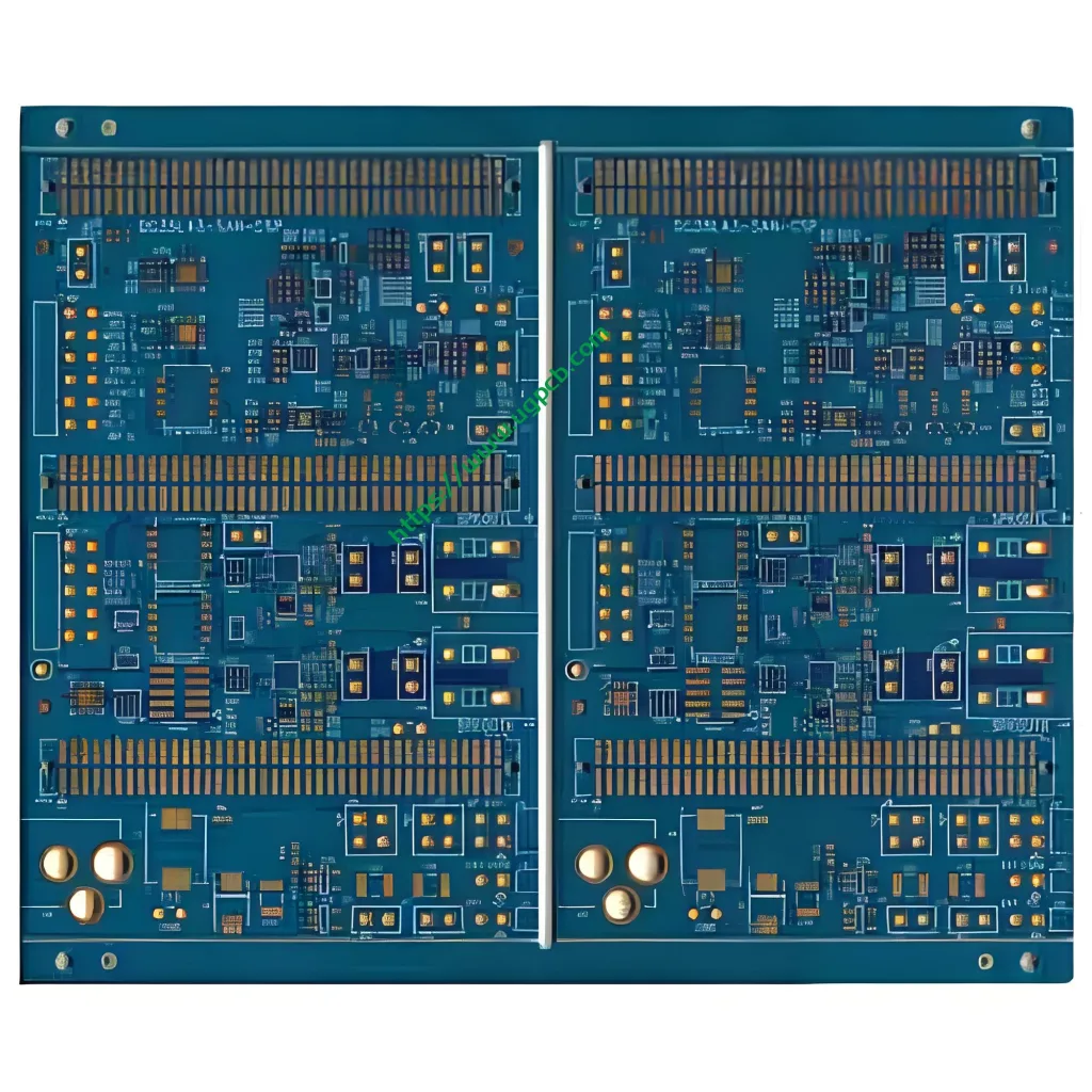
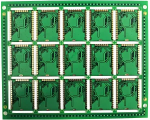
General Guidelines
Ground Planes
에이. Ground planes are preferred because of their ability to route signals in a microstrip configuration.
Low Impedance and Low Noise
비. Ground plane based 12-layer PCB with low ground impedance and low noise.
High-Speed Signal Tracing
기음. The middle layer between layers is used as the trace for high-speed signals. Even in adjacent planes, the signal layers must be tightly packed with each other.
Adjacent Layer Placement
디. You must place the plane and signal layers in adjacent layers.
Tight Coupling of Planes
이자형. The large plan and power planes are tightly coupled together.
Expert Design Team Focus
Signal Layer Adjacent to Plane
- The signal layer should always be adjacent to the plane.
Power Plane as Return Path
- The power plane can be used for the return path of the signal.
Tight Coupling of Signal Layers
- Signal layers should be tightly coupled to their adjacent planes.
Determining Signal Return Portion
- Determine the return portion of the signal.
 UGPCB 로고

