재료 구성
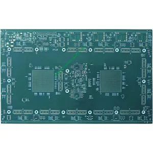
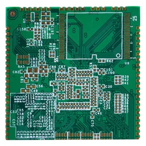
The 2L WiFi Bluetooth Module is crafted from high-quality FR4, a flame-retardant grade of epoxy glass cloth that offers exceptional electrical, 기계적인, 및 열 특성. This material ensures durability and reliability in various environmental conditions.
공사 내용
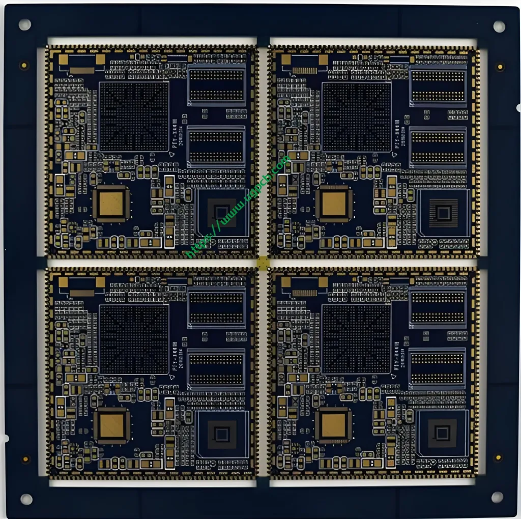
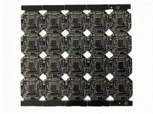
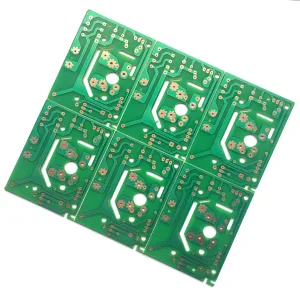
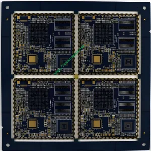
With a sleek design, the module features a 2-layer construction, available in black or white color options. The finished thickness of the PCB is 1.0mm, providing a sturdy base for the electronic components. 1oz의 구리 두께 (온스) per square foot guarantees efficient heat dissipation and signal transmission.
표면 마감
To enhance conductivity and corrosion resistance, the surface of the 2L WiFi Bluetooth Module undergoes immersion gold treatment. This process coats the copper traces with a thin layer of gold, ensuring a high-quality electrical connection and long-term stability.
Manufacturing Precision
Precision is key in the production of the 2L WiFi Bluetooth Module. With a minimum trace width and spacing of 4mil (0.1mm), the PCB supports intricate circuit designs while maintaining optimal electrical performance. 추가적으로, the half-hole PCB characteristic allows for versatile component mounting and enhanced circuit integration.
생산 워크 플로
The production of the 2L WiFi Bluetooth Module involves several meticulous steps:
- Design Layout: The initial phase involves creating the PCB layout using specialized software, ensuring all electrical and physical requirements are met.
- 재료 준비: High-quality FR4 sheets are cut to size and prepared for the manufacturing process.
- 회로 에칭: Using advanced etching techniques, the copper traces are precisely etched onto the FR4 substrate.
- 시추 및 도금: Holes are drilled for component mounting, and the surface is plated with immersion gold to enhance conductivity.
- 품질 관리: Each PCB undergoes rigorous testing to ensure it meets the required specifications.
- 집회: 마지막으로, the PCB is assembled with the necessary components to form the complete 2L WiFi Bluetooth Module.
응용 시나리오
The versatility of the 2L WiFi Bluetooth Module makes it ideal for a wide range of applications:
- Smart Home Devices: Integrate seamlessly into smart home systems, enabling wireless control and monitoring.
- IoT 제품: Perfect for Internet of Things devices that require reliable WiFi and Bluetooth connectivity.
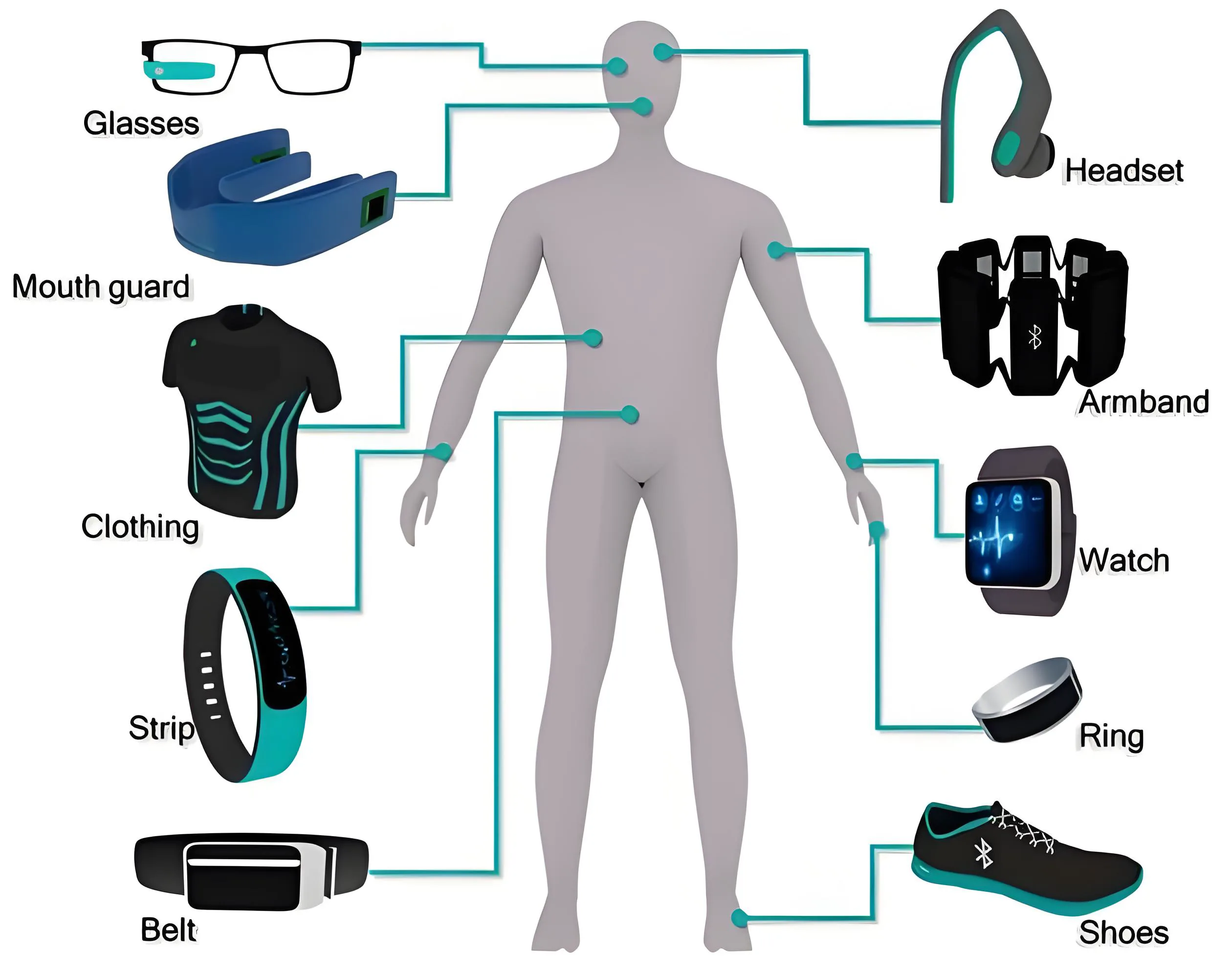
- 웨어러블 기술: Enhance the functionality of wearable devices with efficient wireless communication capabilities.
- 산업 자동화: Facilitate machine-to-machine communication in industrial settings, improving operational efficiency.
결론적으로, the 2L WiFi Bluetooth Module combines superior material quality, precise manufacturing, and versatile application possibilities, making it an excellent choice for developers and engineers seeking reliable wireless connectivity solutions.
 UGPCB 로고

