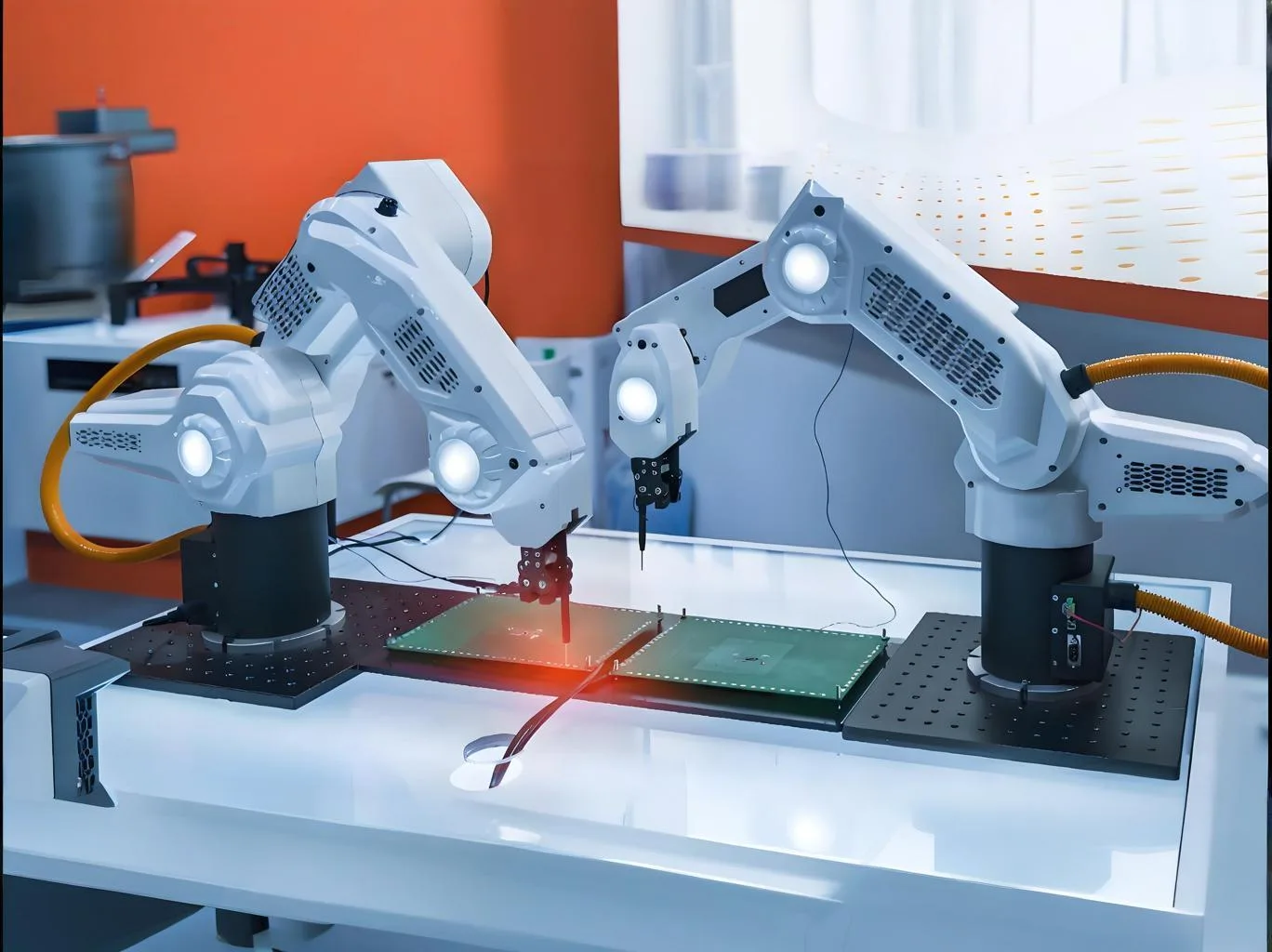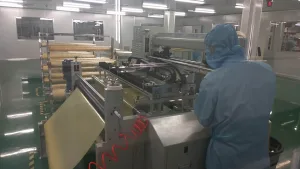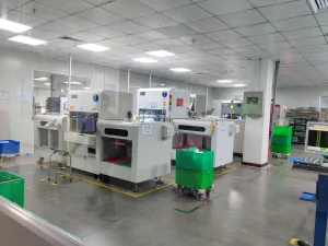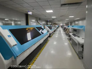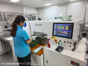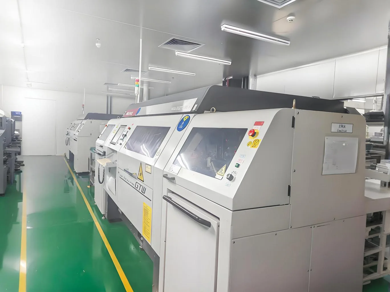
Mitsubishi PCB 레이저 드릴링 머신은 고급 회로 보드 제조의 핵심 장비이며 상당한 투자를 통해 UGPCB가 도입 한 주요 PCB 생산 시스템 중 하나입니다.. Designed for processing micro-vias in precision PCBs such as 고밀도 상호 연결 (HDI) 무대 그리고 IC 기판, it utilizes UV/CO₂ laser technology to accurately ablate PCB materials, creating blind vias and through-holes as small as 30μm in diameter. This capability addresses the growing demand for miniaturization and high-precision interconnects in 5G communications, 가전제품, and related fields. 추가적으로, it enables rapid prototyping and small-batch production of advanced PCBs.
Core Function
The machine’s primary role is to achieve micron-level precision in via formation, ensuring reliable electrical connections in multilayer boards while maintaining structural integrity.
주요 특징
Ultra-High Precision
Equipped with optical positioning and dynamic focusing technologies, the machine achieves a drilling positional accuracy of ±10μm. It adapts to complex laminated materials (예를 들어, 구리, 수지) and heterogeneous layer structures.
High Efficiency
By employing multi-beam parallel processing, it delivers a drilling speed exceeding 200,000 holes per hour, significantly boosting production capacity for high-volume orders.
Intelligent Control
An integrated real-time monitoring system automatically optimizes laser energy output, minimizing issues such as overburning or residual glue, thereby ensuring consistently high yields.
Robust Durability
Built-in temperature control and dust removal modules enable 24/7 continuous operation with minimal downtime. The design emphasizes ease of maintenance and long-term reliability.
Energy Efficiency
With optimized laser utilization, the system reduces energy consumption by 30% compared to traditional mechanical drilling methods, aligning with global green manufacturing standards.
Impact and Significance
Combining 고속, precision, and low material loss, the Mitsubishi PCB Laser Drilling Machine has become indispensable for mass production of advanced PCBs. It drives the evolution of electronic components toward smaller form factors, higher density, and enhanced reliability, cementing its role as a cornerstone of next-generation electronics manufacturing.
 UGPCB 로고
