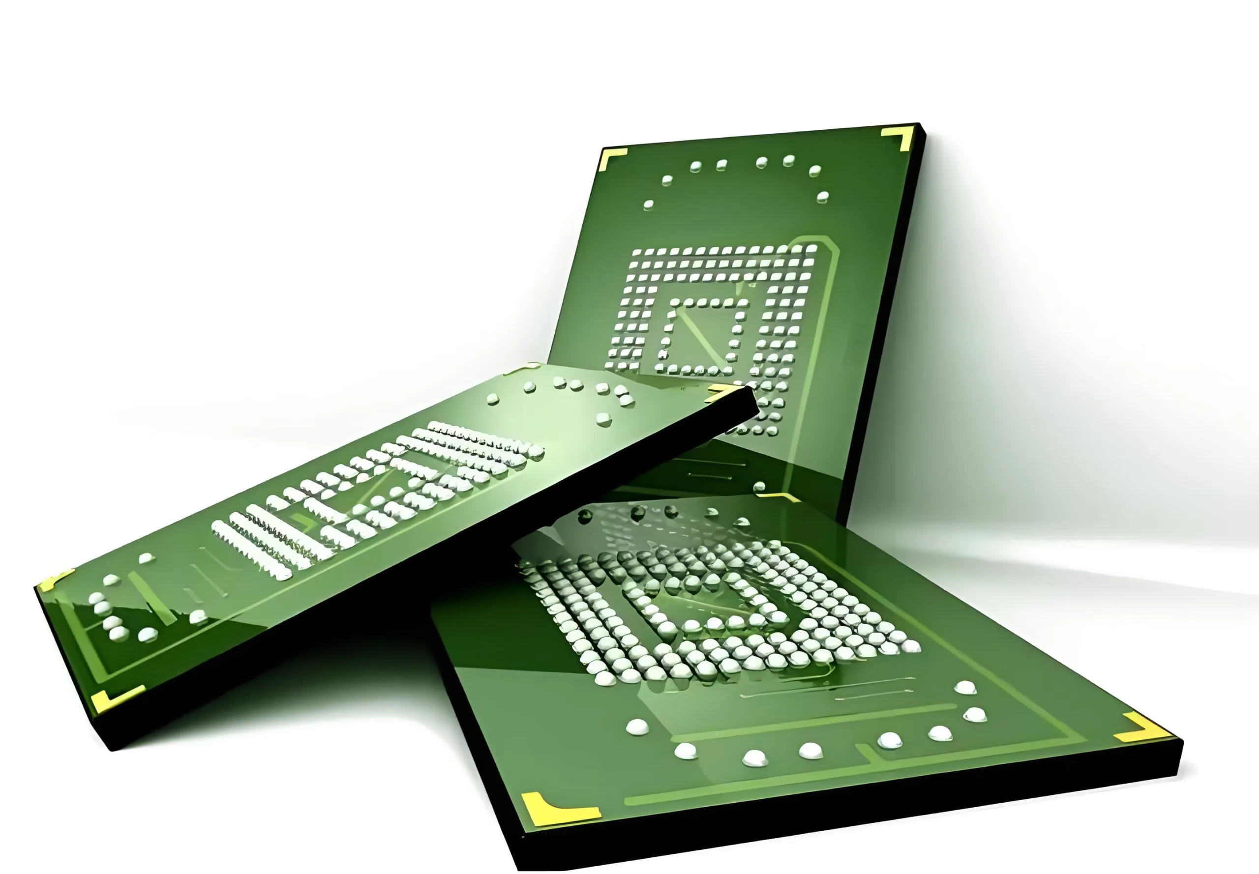
BGA defect and failure analysis.
This article identifies possible assembly anomalies related to the assembly of BGA components. It describes post-process failures related to the characteristics of the mounting structure as well as variations in solder balls used as BGA terminals. In many cases, if the features are attributed to connection point failures, a special discussion on the metallography of the connectors is required. The final connection point structure is also analyzed.
1.Solder Resist Defined BGA Conditions
BGA pads are defined in two ways: Solder Resist Defined (SMD), where the pad size is larger than the opening in the solder resist, allowing the molten BGA solder ball to contact the solder resist after reflow soldering; and another method called etched or Non-Solder Resist Defined (NSMD), where the solder resist opening is larger than the copper pad, so the solder ball does not contact the solder resist after reflow soldering. See sections 1.1 and 1.2 for details.
1.1 Solder Resist Defined vs. Non-Defined Pads
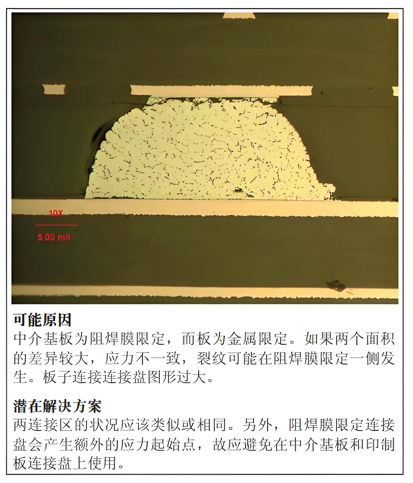
The reasons and solutions for the appearance of solder resist defined and non-defined pads
1.2 Solder Resist Defined Pads on Product Boards
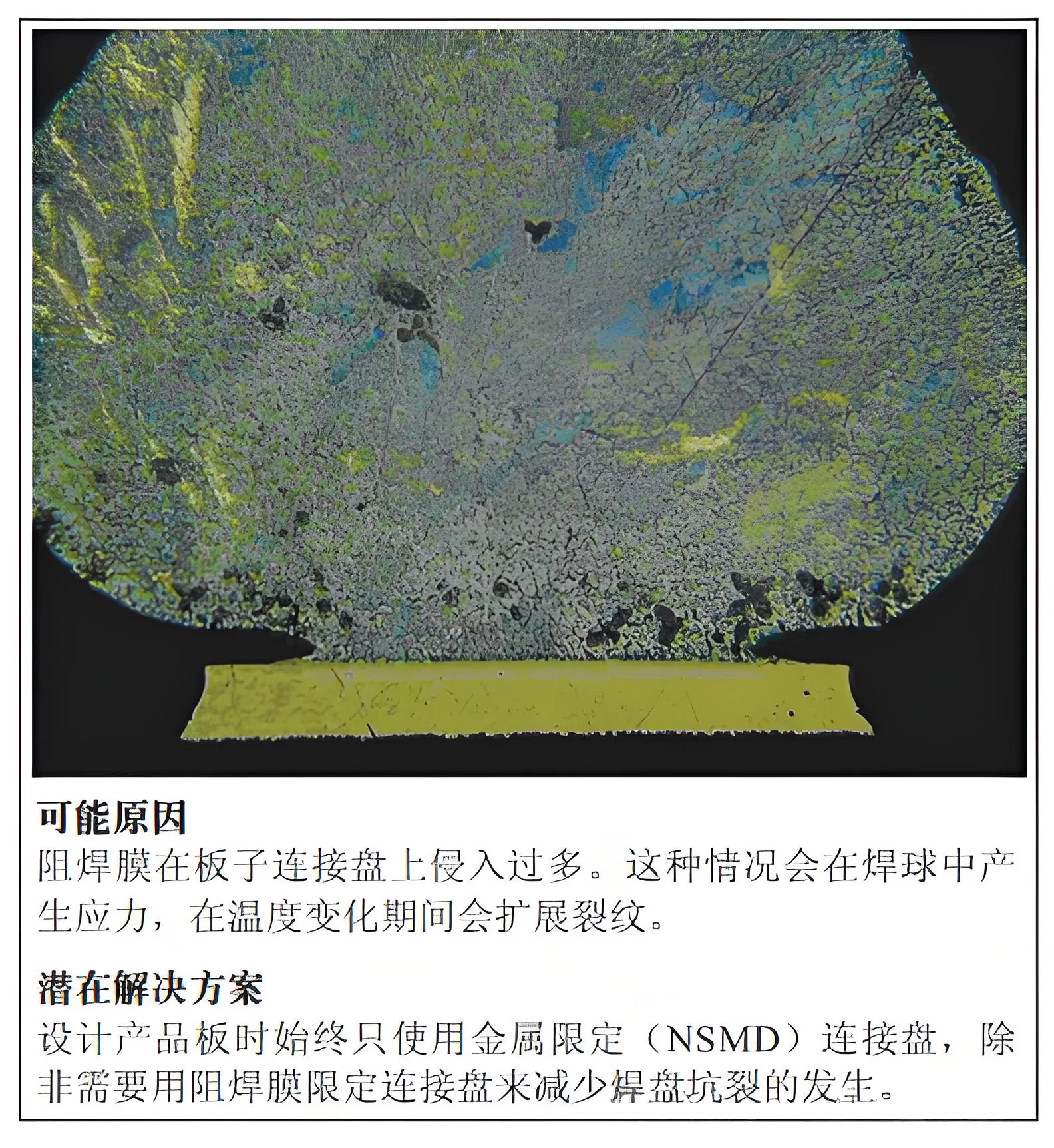
Analysis and Solution for the Causes of Solder Resist Limiting Pads on PCB Boards
Solder resist defined pads can be used on corresponding non-critical or functional pins because SMD pads can help minimize the defect of pad cratering. However, it should be noted that solder resist defined connections generate additional stress initiation points and should be avoided on interposer substrates and PCB pads.
The main disadvantage of solder resist defined pads lies in the stress concentration generated by SMD (Solder Resist Defined) solder joints, which becomes the origin of solder joint failure and reduces reliability. As shown in point 3 below, for the same solder joint height, the fatigue life factor when using Non-Solder Resist Defined (NSMD) increases by an estimated 1.25 to 3 times compared to SMD pads, with greater improvements under more stringent load conditions.
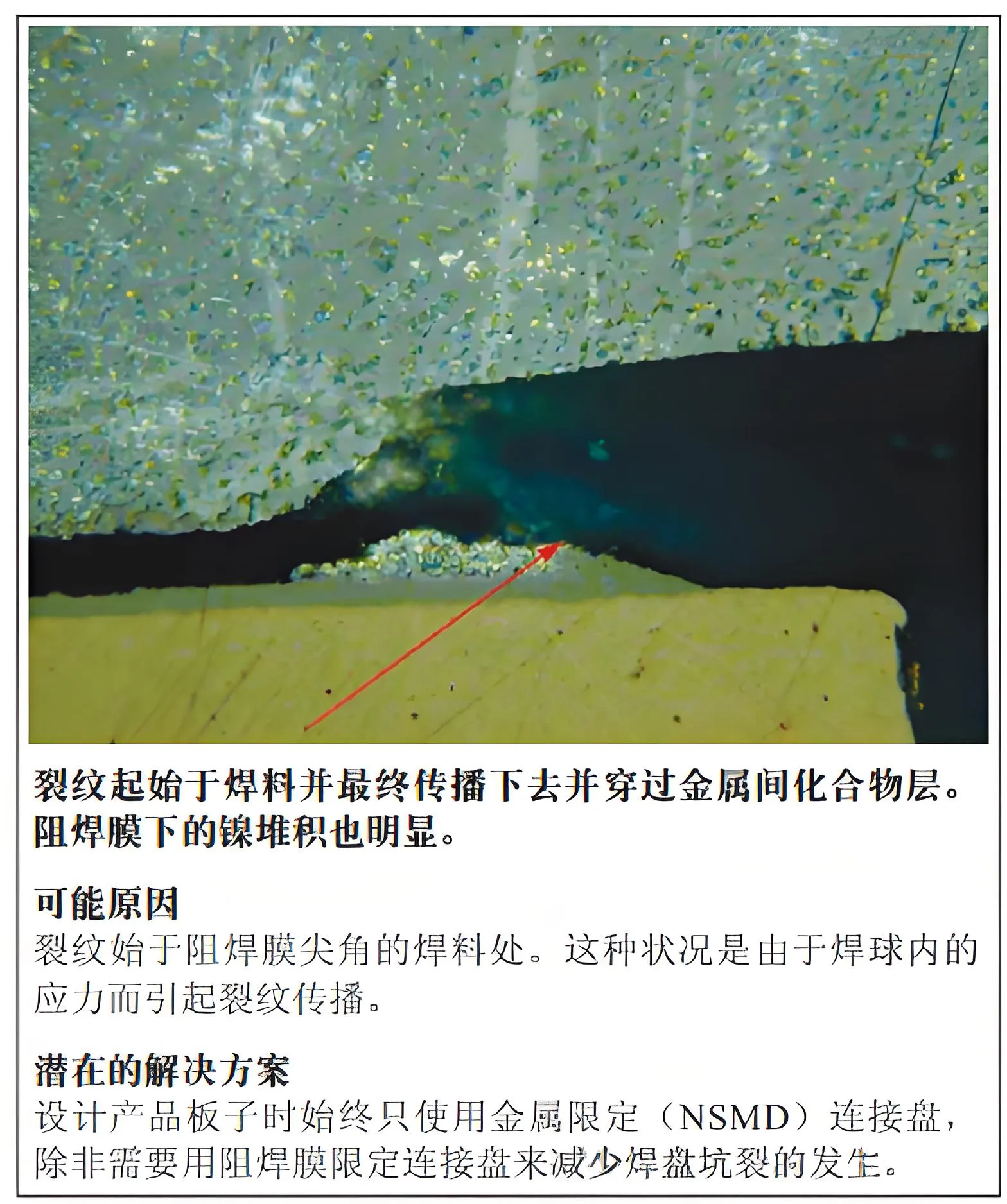
Causes and solutions for cracks in SMD solder joints
SMD pads have three main disadvantages
- Less substrate area causing top separation
- Loss of pad size accuracy
- Reduced reliability, as it is the origin of early failure in solder joints
2.Excessive Collapse of BGA Solder Balls
Molded BGA solder balls typically collapse from their original size of 750μm to about 625μm. After the package is soldered to the board, the solder balls collapse to about 500μm. However, if there are heat sinks or thermal blocks inside the package, the solder balls may collapse down to 300μm. When the solder balls flatten, their reliability decreases due to the limited solder height and flexibility of the solder joints. Also, the extension of the solder balls may exceed the expected pitch gap. A better approximation is an initial reflow reduction of about 10% height; with the added weight of heat sinks, this number may increase to 25% of the original height (solder ball diameter). The pattern of the connection pads and the gap in the solder resist also play a role in the analysis. The extreme values of this situation are shown in sections 2.1 to 2.4.
2.1 BGA Solder Ball without Heat Sink, 300μm Holding Height

The cause and solution for the collapse of BGA balls without a heat dissipation block
2.2 BGA Solder Ball with Heat Sink, 375μm Holding Height

The reason and solution for the spherical collapse of BGA with heat sink
2.3 BGA Solder Ball with Heat Sink, 300μm Holding Height
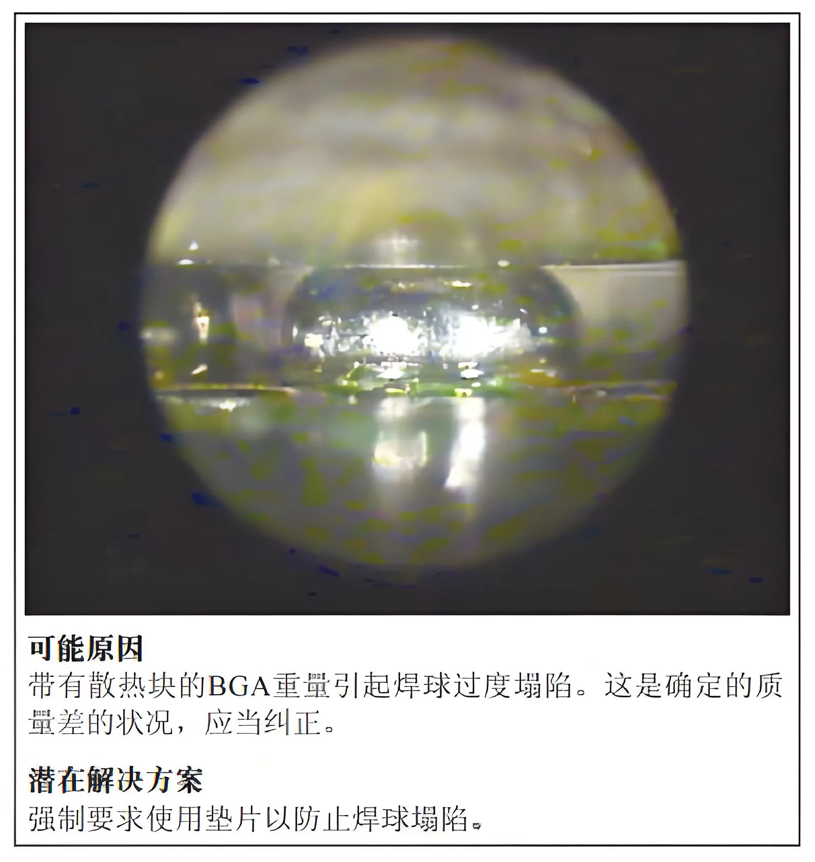
The reason and solution for the spherical collapse of BGA with heat sink
2.4 Critical Solder Paste Conditions
The amount of deposited solder paste is helpful for molded BGA connections but is not very critical for the formation of good solder joints, as the solder balls themselves can act as a source of solder. However, for Ceramic BGA (CBGA), depositing sufficient solder paste is very important. For an 890μm CBGA, the recommended amount of solder paste is 0.12mm³, at least 0.08 mm³. If not enough solder paste is deposited, as shown in section 3.1, the reliability of the solder joint may be problematic. Solder must be added to high-temperature solder balls or posts because the volume of solder from the package terminal does not contribute to the solder joint.
2.5 Excessive Thick Paste Deposition
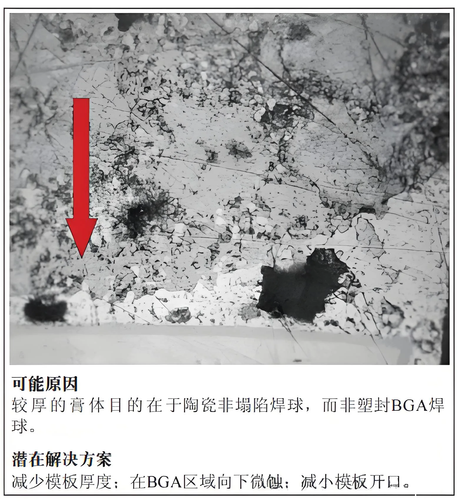
Causes and solutions for excessive paste deposition
2.6 Void Detection through X-ray and Sectioning
Transmission X-ray can detect the presence of voids (light areas) and related X-Y positions. This technique can also detect uneven or missing solder balls (various dark image diameters), examples of which are shown in section 2.7. However, X-ray sectioning is needed to determine the vertical (Z-axis) position of voids in the solder joint.
2.7 Voids and Uneven Solder Balls
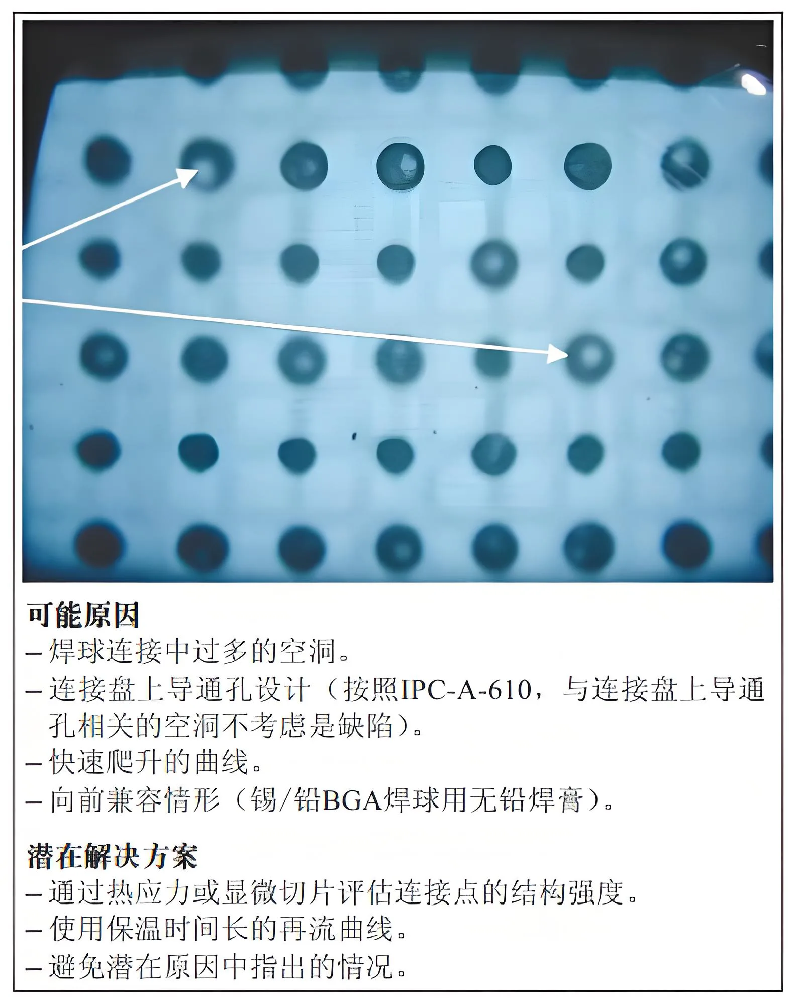
Hollow and non-uniform solder balls and solutions
There are many reasons for the formation of voids in BGAs. Although more common voids are shown in section 2.7, voids do not pose any reliability risk. Voids like those shown in section 2.8 can withstand 1000 thermal cycles (no shock, 0-100°C). Even in some tests, voids do not reduce fatigue life results, excessive voids in solder joints indicate issues with design, process, or materials. Product reliability should also be verified.
2.8 Eggshell Voids
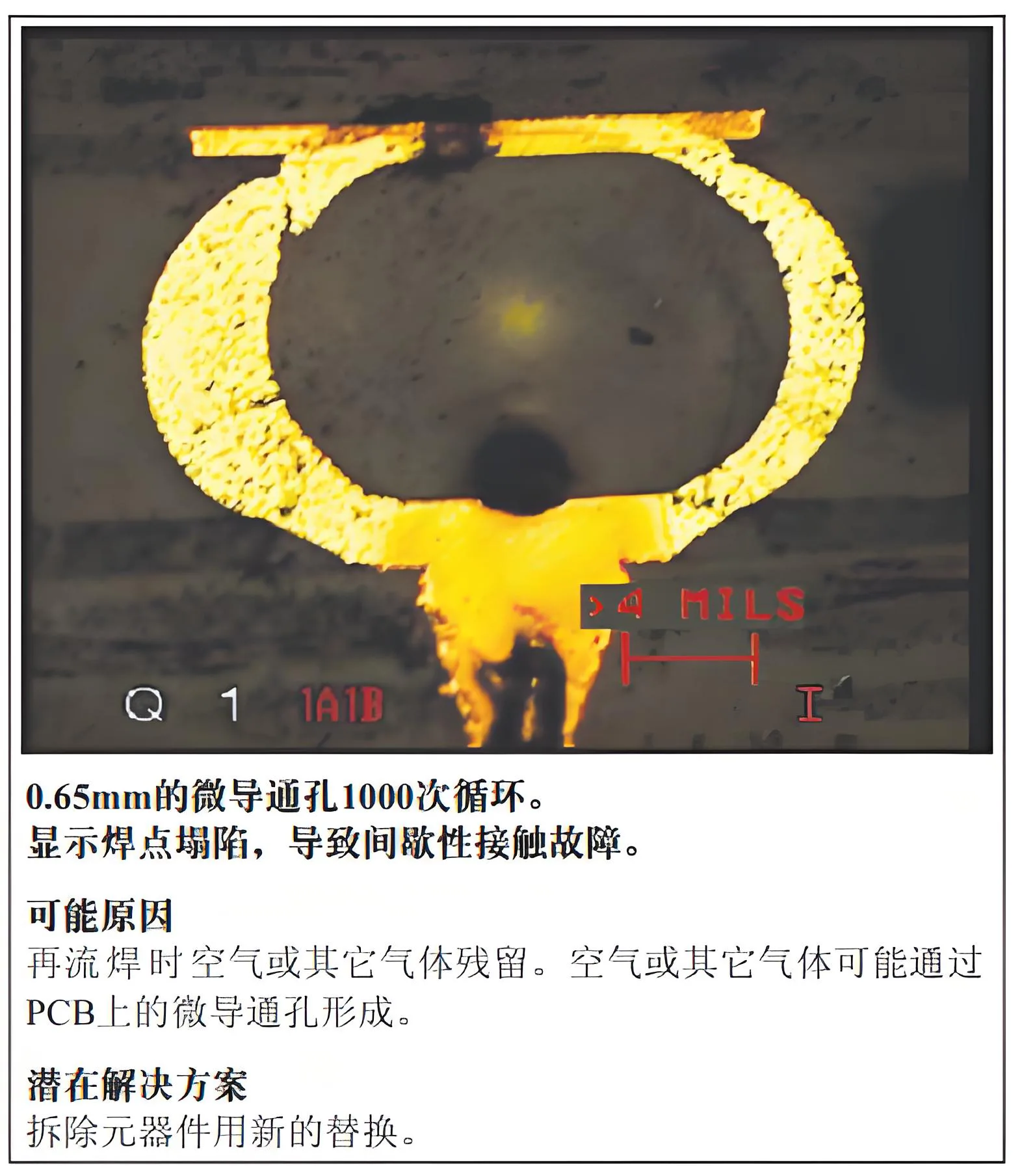
The causes and solutions for eggshell porosity
3.Warpage and Distortion of BGA Substrates
In normal assembly reflow processes, molded BGAs tend to warp. Warpage can occur on the BGA substrate or product PCB. The result is stressed solder joints becoming open or short circuit conditions. Temperature (reflow profile), BGA structure, solder paste volume, and cooling conditions all bring potential defects. Corner solder ball shorts are an indication of BGA warpage, with the corners of the BGA package warping inward (crying BGA).
Solder shorts occur between adjacent and/or opposite BGA corners due to substrate downward bending (crying face), stressing the corner solder balls. The same phenomenon causes solder balls far from the corners to lift away from the mounting substrate, as the substrate changes from a crying face to a smiling face, as shown in sections 3.1 and 3.2. As BGA substrates and chips become thinner, warpage of the package also increases. To have a robust SMT process, it is recommended to check if sufficient solder paste has been added to the connection pads. This process should be closely monitored to ensure no additional defects such as solder bridges or beads occur.
3.1 BGA Interposer Substrate Warpage
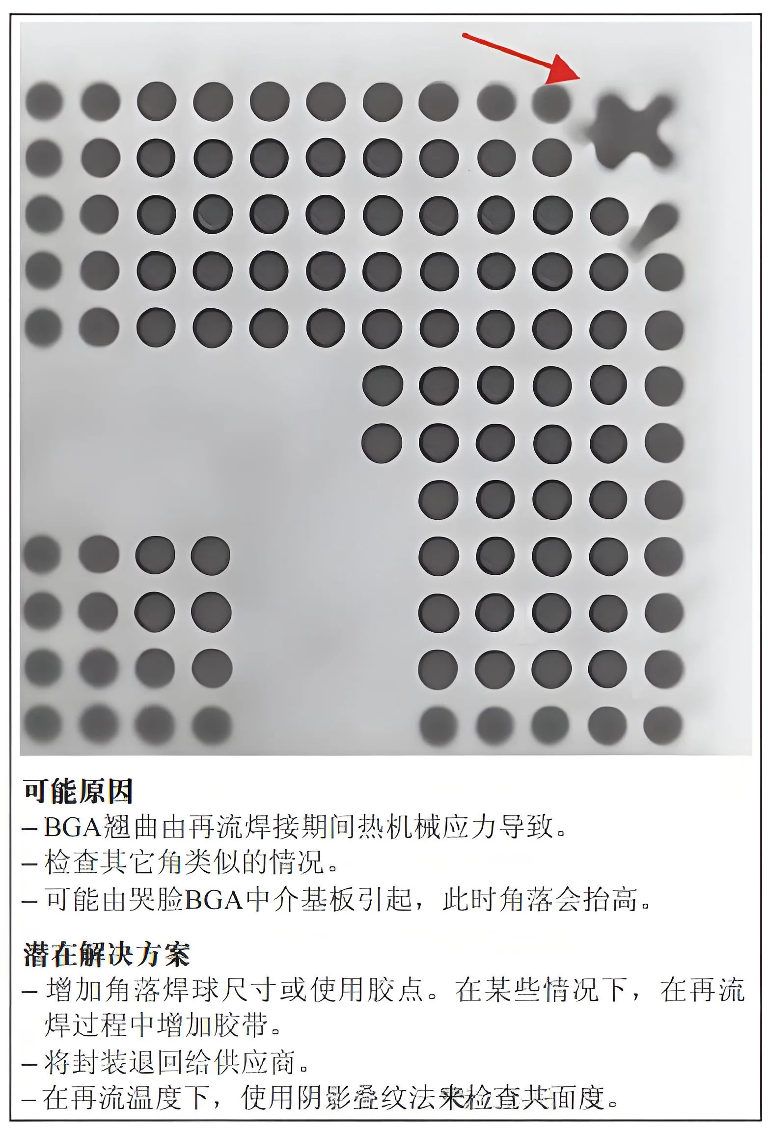
Open circuits of corner solder balls are an indication of BGA warpage, with the package corners lifting upwards. This open circuit, as shown in section 3.2, can be minimized by using additional solder paste volume.
3.2 Solder Joint Open Circuit Due to Interposer Substrate Warpage
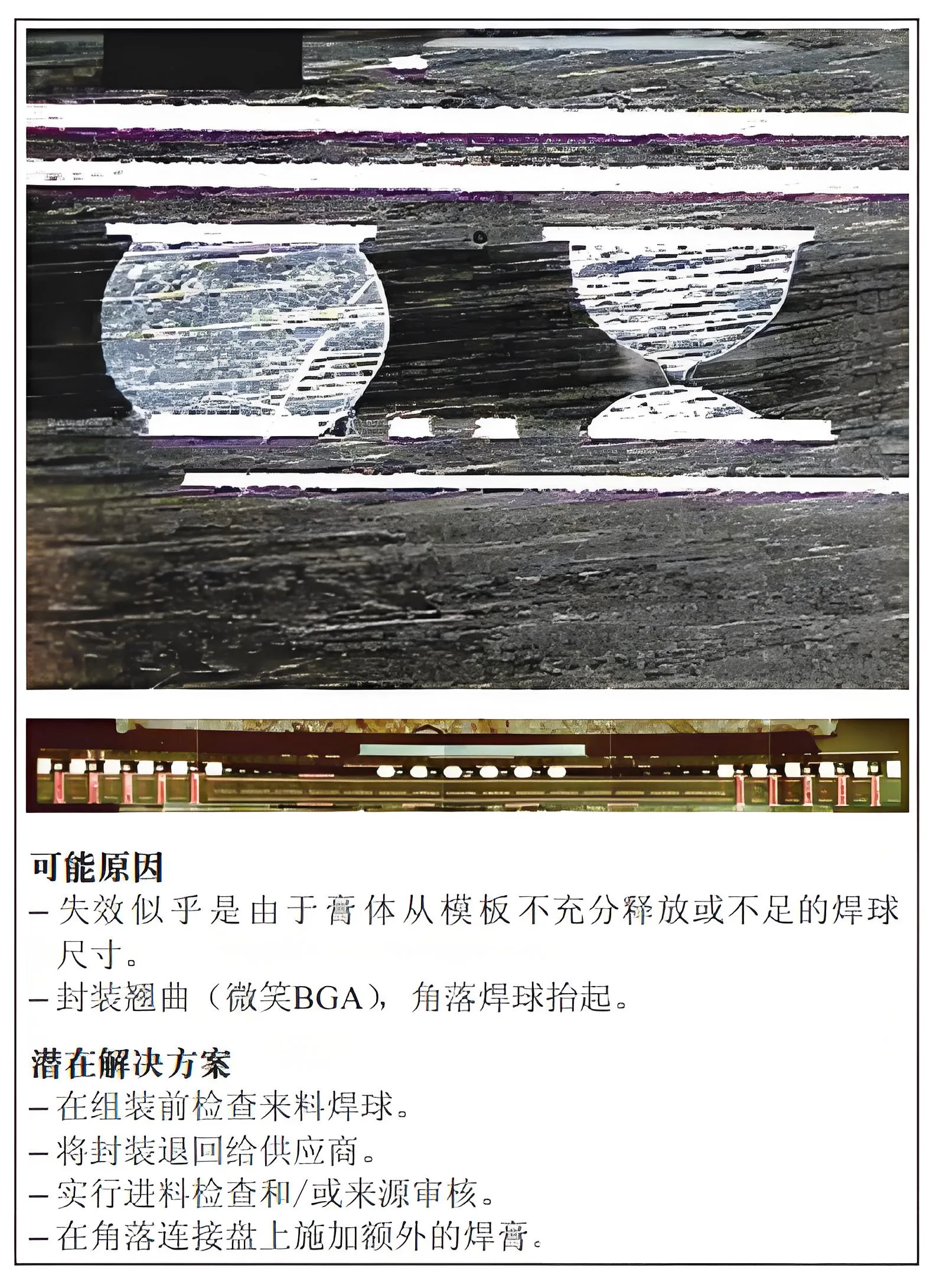
The reason and solution for open circuit caused by PCB warpage
Applying excess solder paste is not a solution to this problem. Identifying the root cause and addressing the anomaly reasons is more important for establishing a robust process. Modifying the stencil opening to deposit solder paste on the board should only be considered as a solution for correcting corner open circuits if a process or component condition cannot be changed, such as if the reflow process has been optimized, the BGA package or BGA interposer substrate cannot be redesigned, or the product board cannot be redesigned. Additionally, anomalies are likely to continue occurring, and before making any process changes, the inventory of solder and components should be considered. If deciding to use excess solder paste to correct corner solder ball open circuits, closely monitor this process to ensure no additional defects such as solder bridges or beads occur.
Solder Joint Conditions
Next, we discuss the conditions of the solder balls associated with the mounting structure and interposer substrate. For each case, explanations are given regarding the causes of this condition.
4.1 Target Soldering Conditions

Causes and Solutions for Open Circuits at Weld Points Due to Targeted Welding Conditions
4.2 Over-Oxidized Solder Balls
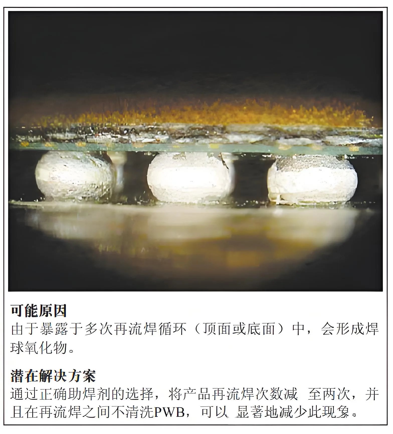
The reason for the open circuit caused by over-oxidized solder balls and its solution
4.3 Signs of Wettability

Reasons for and Solutions to Solder Joint Open Circuits Caused by Dewetting
4.4 Spotted Conditions

The cause and solution of solder joint defects caused by solder ball spots
4.5 Tin/Lead Solder Ball Assessment
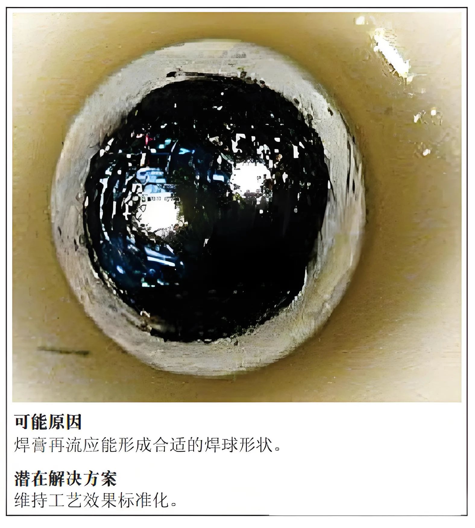
Reasons and Solutions for Solder Joint Defects Caused by Tin/Lead Solder Balls
4.6 SAC Alloy
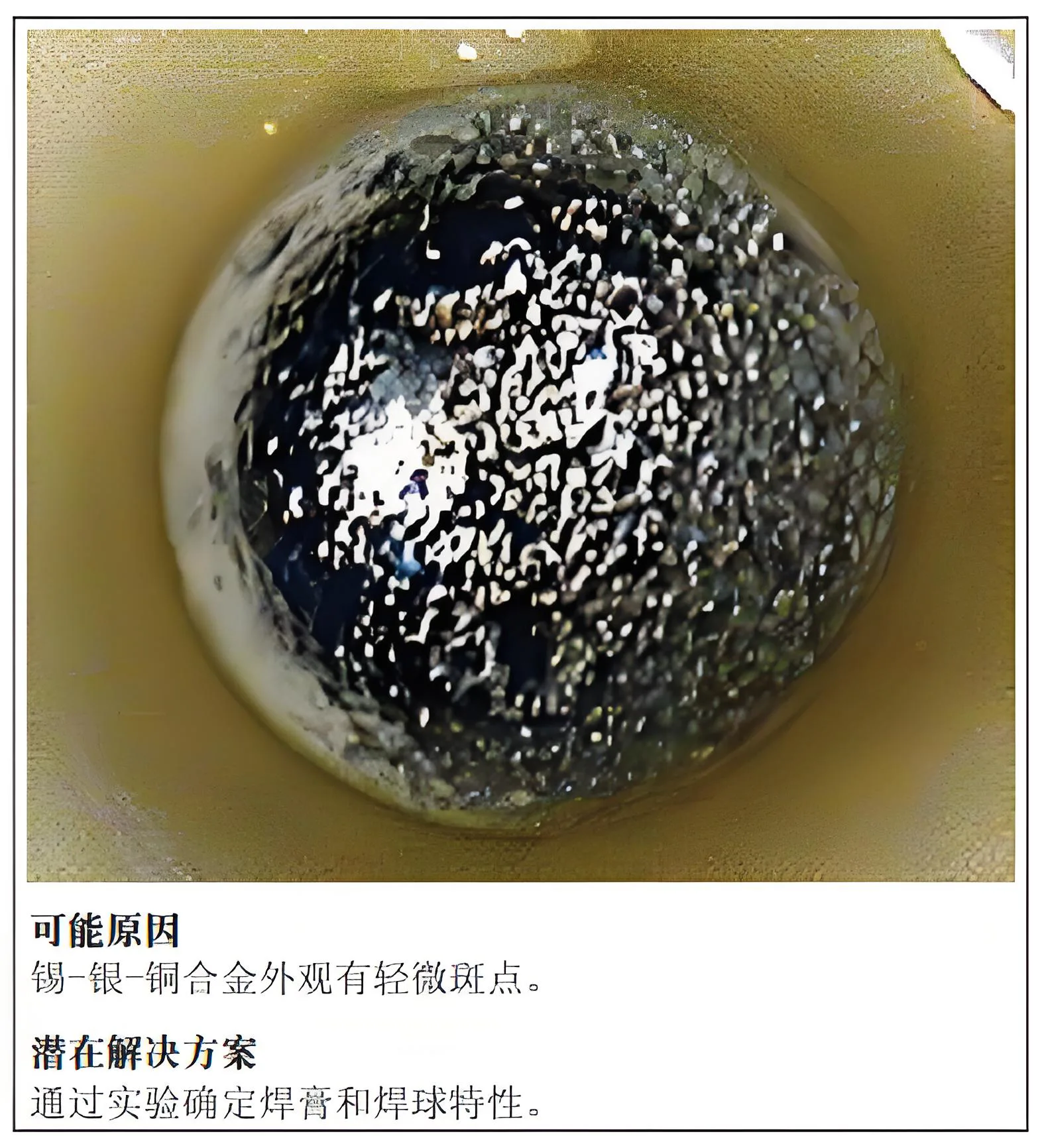
The reasons and solutions for solder joint defects caused by SAC alloy
4.7 Cold Solder Joints
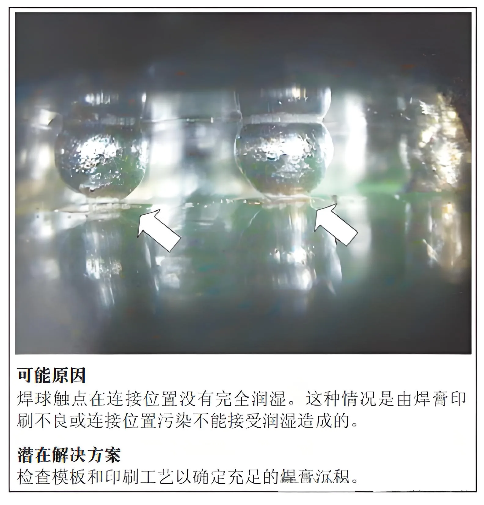
Cold solder points caused by cold solder and their solutions
4.8 Incomplete Joints Caused by Pad Contamination

Causes and solutions for incomplete connections due to contamination of the connecting disk
4.9 Contamination Caused by Deformed Solder Balls
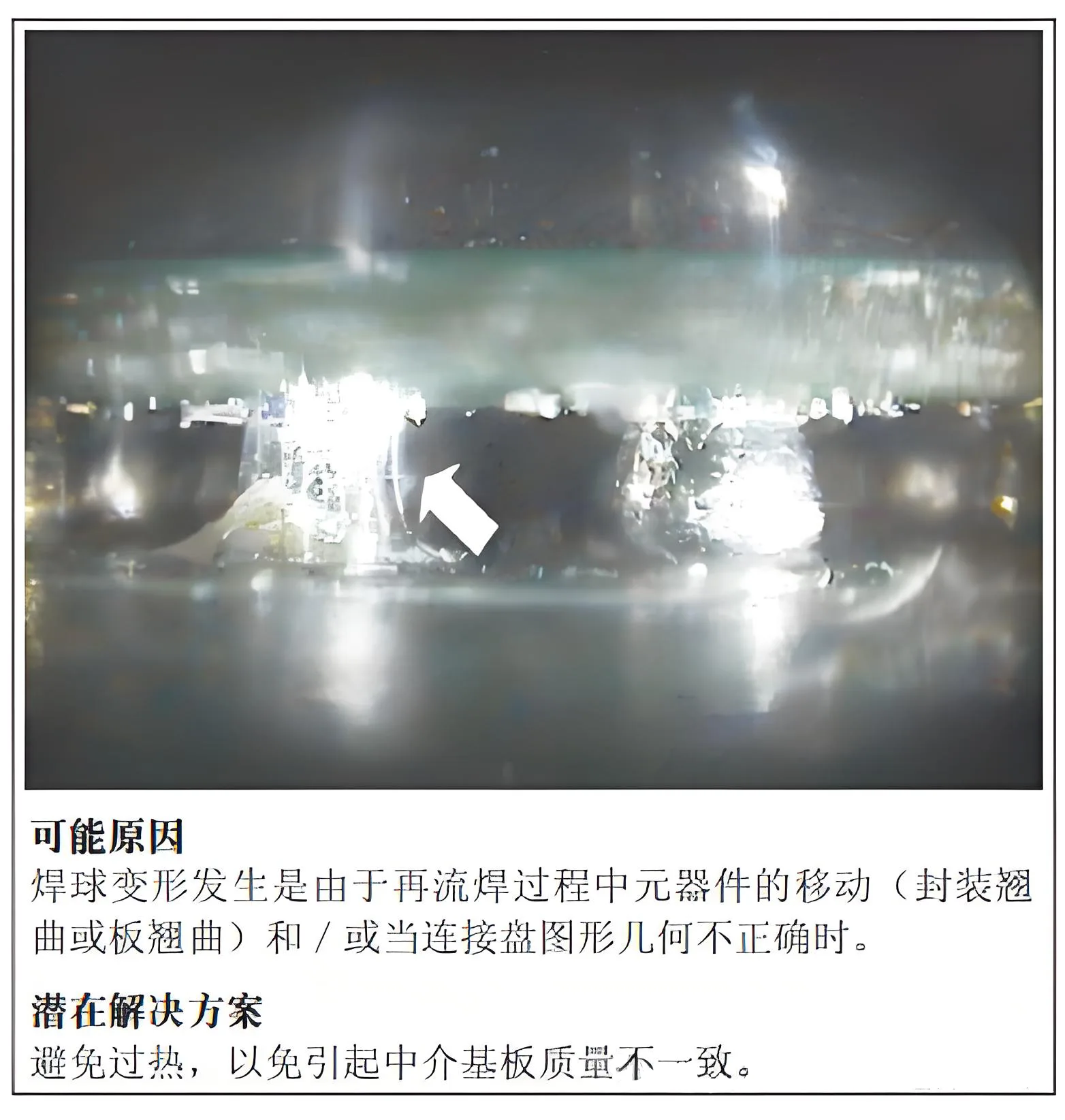
The cause and solution of solder joint defects due to contamination from deformed solder balls
4.10 Deformed Solder Balls
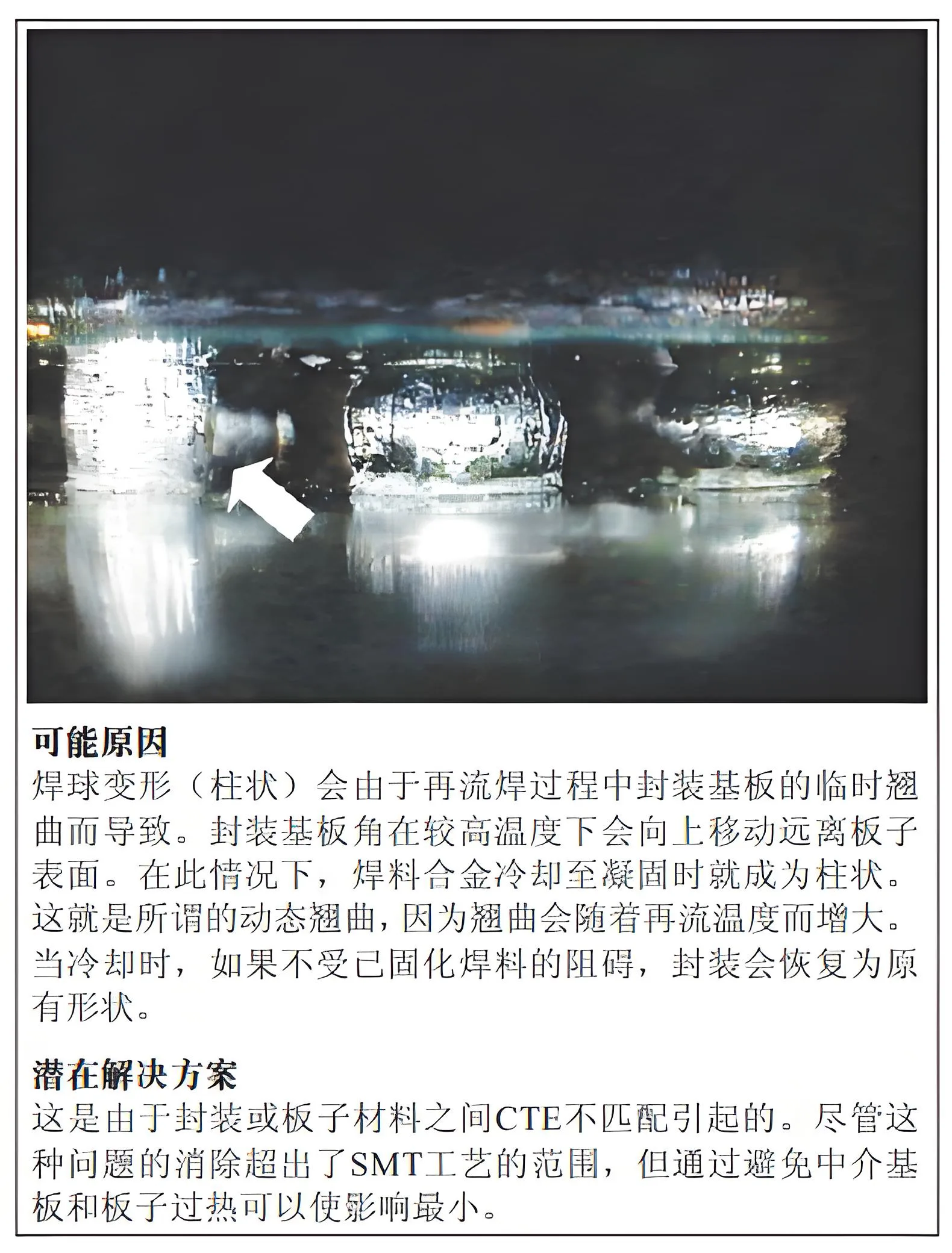
Causes and solutions for solder joint defects caused by deformed solder balls
4.11 Insufficient Solder and Flux for Adequate Joint Formation
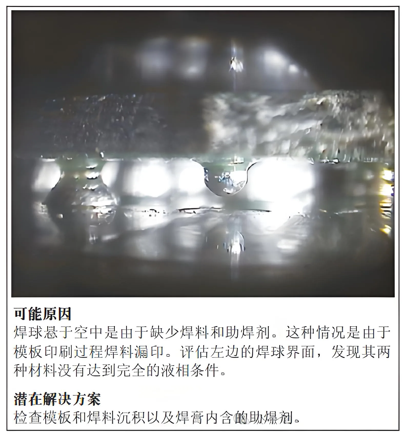
The causes and solutions for solder joint defects caused by insufficient solder and flux
4.12 Reduced Contact Area of Terminals

Reasons for solder joint defects caused by reduced terminal contact area and solutions
4.13 Solder Bridges
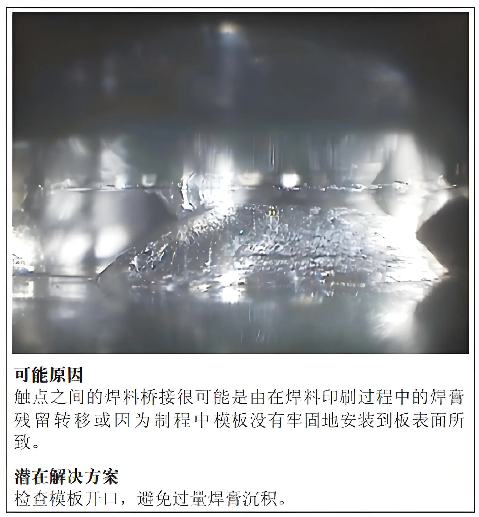
4.14 Incomplete Solder Reflow
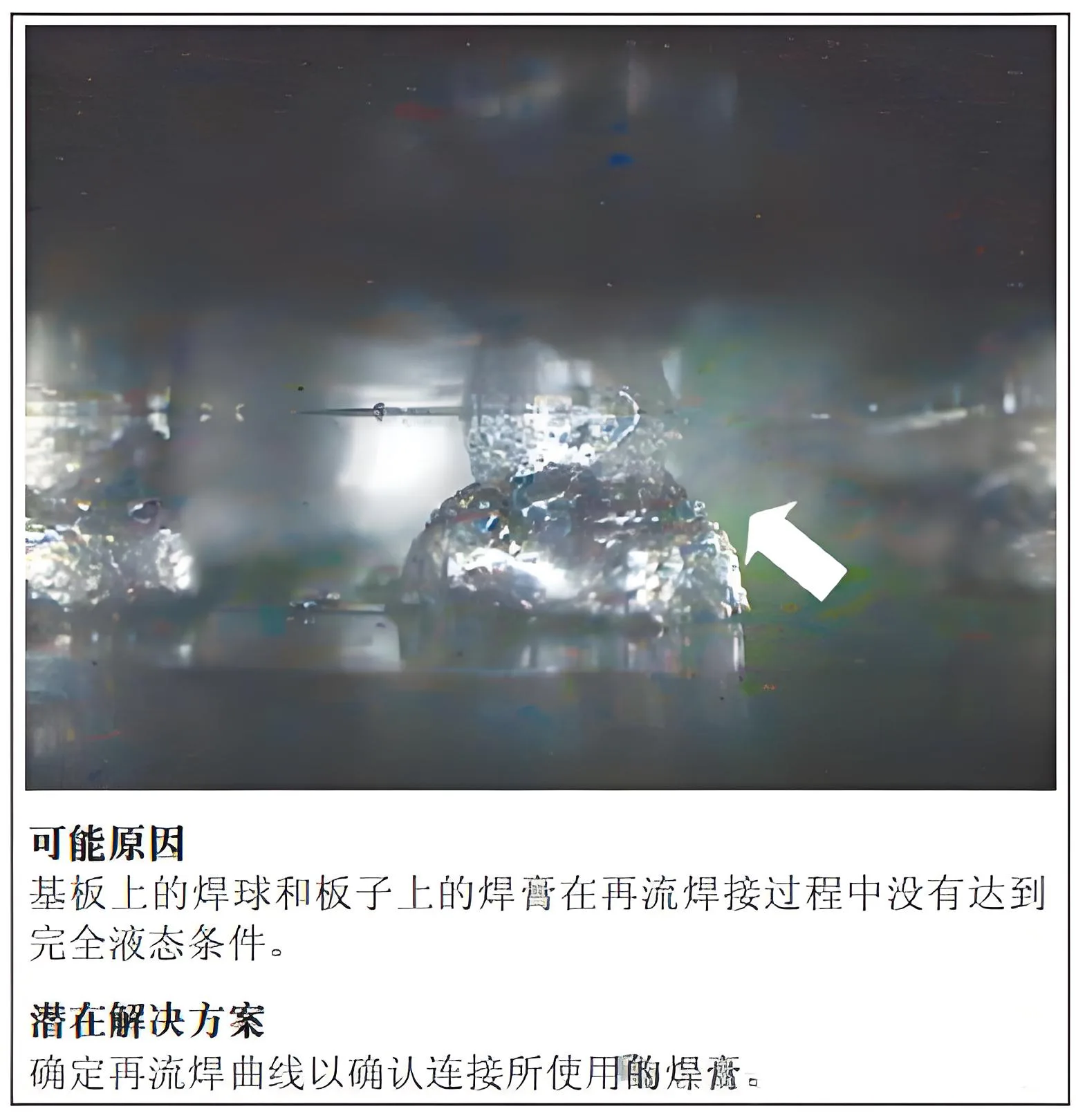
Reasons and Solutions for Solder Joint Defects Caused by Solder Reflow
4.15 Dry Solder Joints
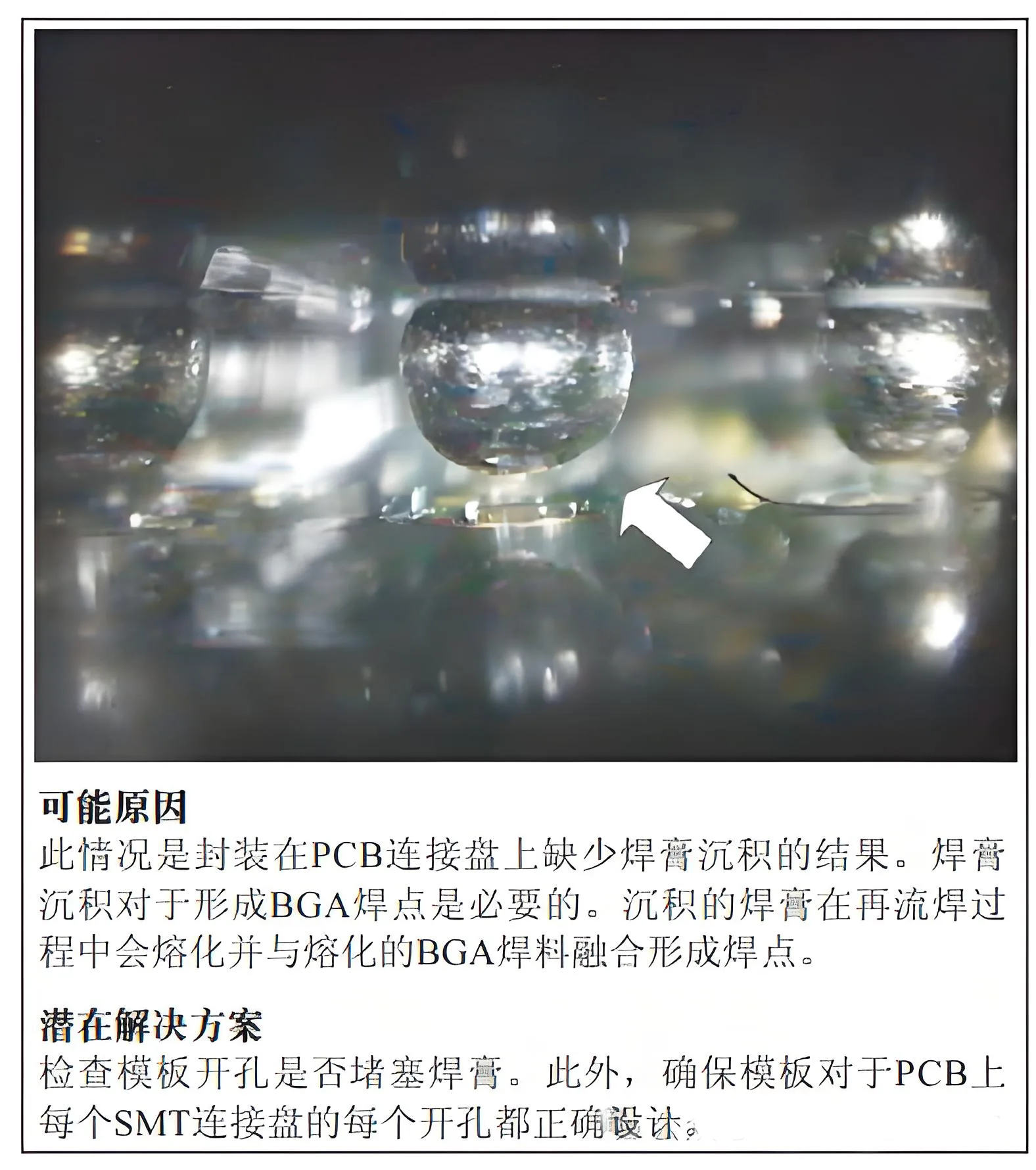
The causes and solutions of solder joint defects caused by empty soldering
4.16 Non-Wetting Solder Joint Open Circuits
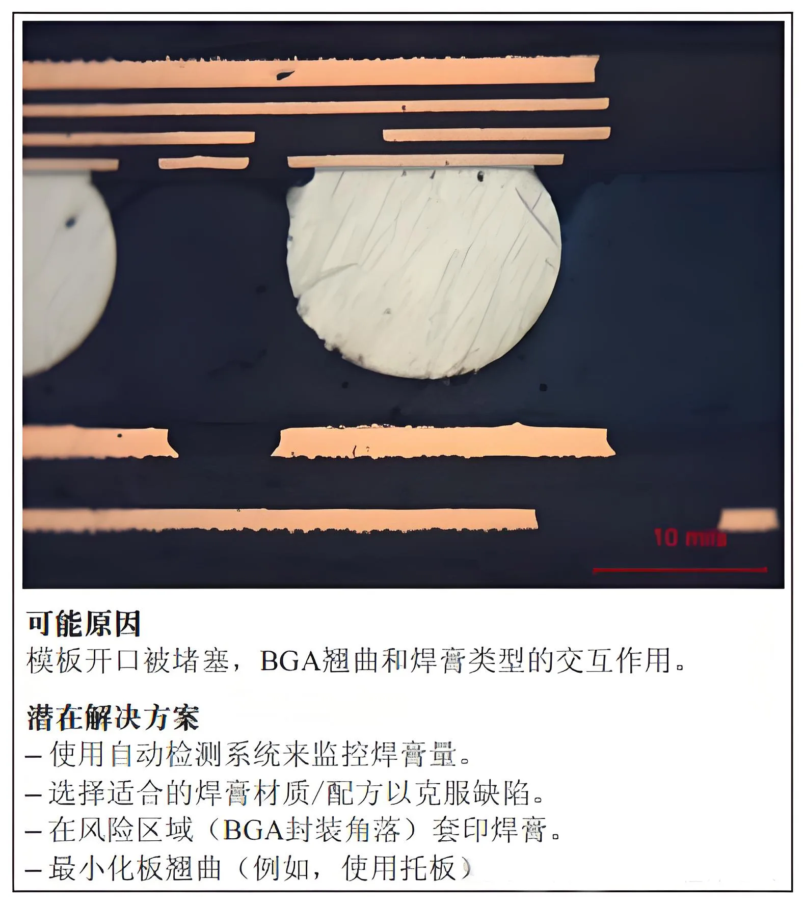
Causes and Solutions for Solder Joint Defects due to Non-wetting Open Circuits
4.17 Pillow Effect Solder Joints (HoP)
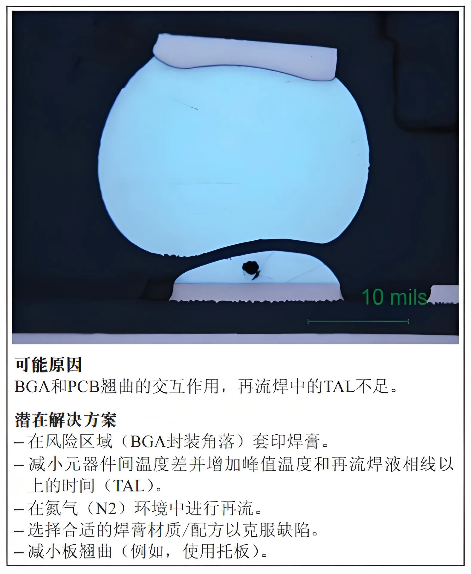
The reason for the formation of pillow effect solder joints and its solution
 UGPCB LOGO

