

In the field of modern electronic engineering, high-power PCB design is undoubtedly a highly challenging task. It not only requires designers to have solid electronic theoretical knowledge but also rich practical experience and exquisite design skills. This article will delve into the preliminary analysis and design techniques of high-power PCB design, helping engineers to navigate this complex field with ease.
I. Overall Design Thinking: Balancing Thermal Management, Electrical Performance, and Mechanical Structure
The core of high-power PCB design lies in ensuring the reliability and stability of the circuit under high current or high voltage conditions. The overall design thinking should focus on the optimization of thermal management, electrical performance, and mechanical structure.
Thermal Management
High-power circuits generate a large amount of heat during operation, so thermal management is of utmost importance in the design. Designers need to evaluate the thermal characteristics of all components, predict hot spots, and design effective heat dissipation paths. For example, using thermal simulation software can predict the thermal distribution of the circuit in advance, thereby optimizing the heat dissipation design.
Electrical Performance
Under high current or high voltage conditions, the stability of electrical performance is crucial. Designers need to consider the voltage and current levels to ensure that the sizes of traces and vias are appropriate. For example, adjusting the trace width according to the current carrying capacity to avoid overheating and voltage drop issues.
Mechanical Structure
The physical size and mounting method of the PCB must be suitable for its working environment. Designers need to ensure that the mechanical structure of the PCB can withstand vibrations, impacts, and temperature changes in the working environment.

II. Preliminary Design Preparation: Requirement Analysis, Component Selection, and Material Selection
Adequate preparation before starting the design is key to success.
Requirement Analysis
Communicate with customers to clarify functional requirements and performance indicators. For example, customers may require the PCB to work stably in high-temperature environments or meet specific electromagnetic compatibility requirements.
Component Selection
Select appropriate components based on their electrical and thermal characteristics. For example, choose components with high voltage and current capacities to ensure the reliability of the circuit.
Material Selection
Choose PCB materials suitable for high-power applications, such as high Tg materials. High Tg materials have a higher glass transition temperature and can maintain stable mechanical and electrical performance in high-temperature environments.
Design Specification Formulation
Determine design standards and testing methods to ensure that the design meets industry specifications. For example, formulate a detailed test plan to ensure that the PCB undergoes strict quality control before leaving the factory.

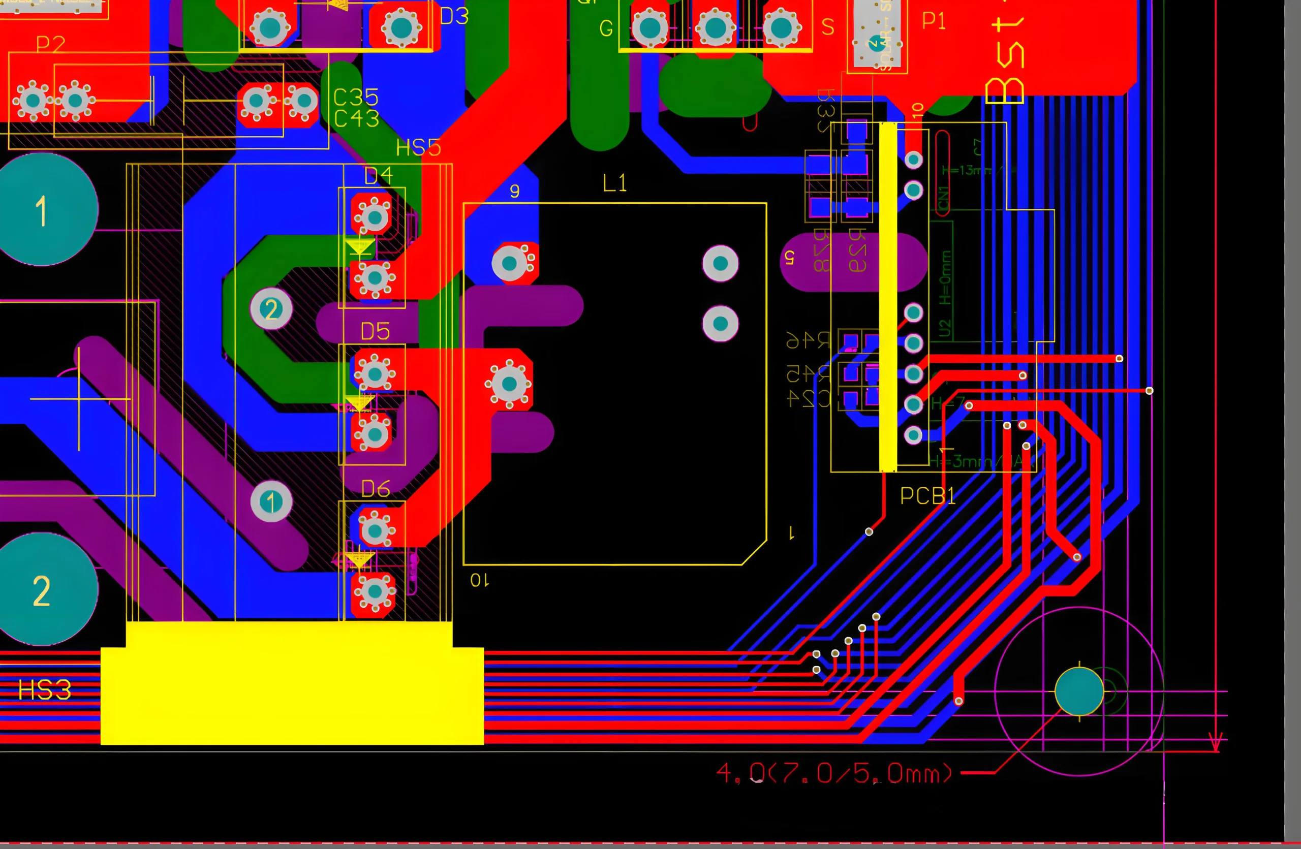
III. Design Techniques During the Design Process: Layout Strategies, Copper Foil Thickness, and Thermal Vias
During the design process, designers need to master a series of design techniques to ensure the reliability and performance of the circuit.
Layout Strategies
Distribute high-power components at the edges of the PCB or in well-ventilated areas to utilize edge cooling. For example, place power MOSFETs at the edges of the PCB for better heat dissipation.
Copper Foil Thickness
Specify a thicker copper foil for key traces and vias to reduce resistance and voltage drops. For example, using 2-ounce copper foil can significantly reduce the resistance of traces and reduce power loss.
Thermal Vias
Use thermal vias in high-power areas to enhance heat conduction. For example, arrange multiple thermal vias under power components to quickly transfer heat to the other side of the PCB.
Trace Width
Adjust the trace width according to the current carrying capacity to avoid overheating. For example, use the following formula to calculate the trace width:

where W is the trace width, I is the current, ρ is the resistivity of copper, L is the trace length, and V is the allowable voltage drop.
Ground Plane and Power Plane
Design complete planes for power and ground to reduce noise and voltage drops. For example, use multilayer PCB design to arrange the power and ground planes on different layers to reduce noise interference.
Shielding and Isolation
Shield sensitive signal lines and perform electrical isolation when necessary. For example, use shielding covers or shielding layers to protect sensitive signal lines from electromagnetic interference.
Simulation Analysis
Use thermal simulation and signal integrity simulation during the design phase to predict potential problems. For example, use simulation software such as ANSYS or Cadence to identify and solve thermal and signal integrity issues in the design in advance.
Modular Design
Decompose complex designs into modules to simplify the design process and improve manageability. For example, design the power module, control module, and signal processing module separately, and then integrate them later.
IV. Common Mistakes and Avoidance Methods: Insufficient Thermal Management, Layout Errors, and Improper Component Placement
When designing high-power PCBs, there are some common mistakes that need to be avoided to ensure the reliability and performance of the circuit.
Insufficient Thermal Management
In high-power PCB design, thermal management is crucial. Ensure effective heat dissipation by using appropriate copper foil thickness, increasing heat dissipation holes, using heat sinks or thermocouples.
Layout Errors
Unreasonable layouts may lead to signal interference and electromagnetic compatibility issues. Give priority to trace routing to ensure an appropriate distance between low-speed and high-speed signals.
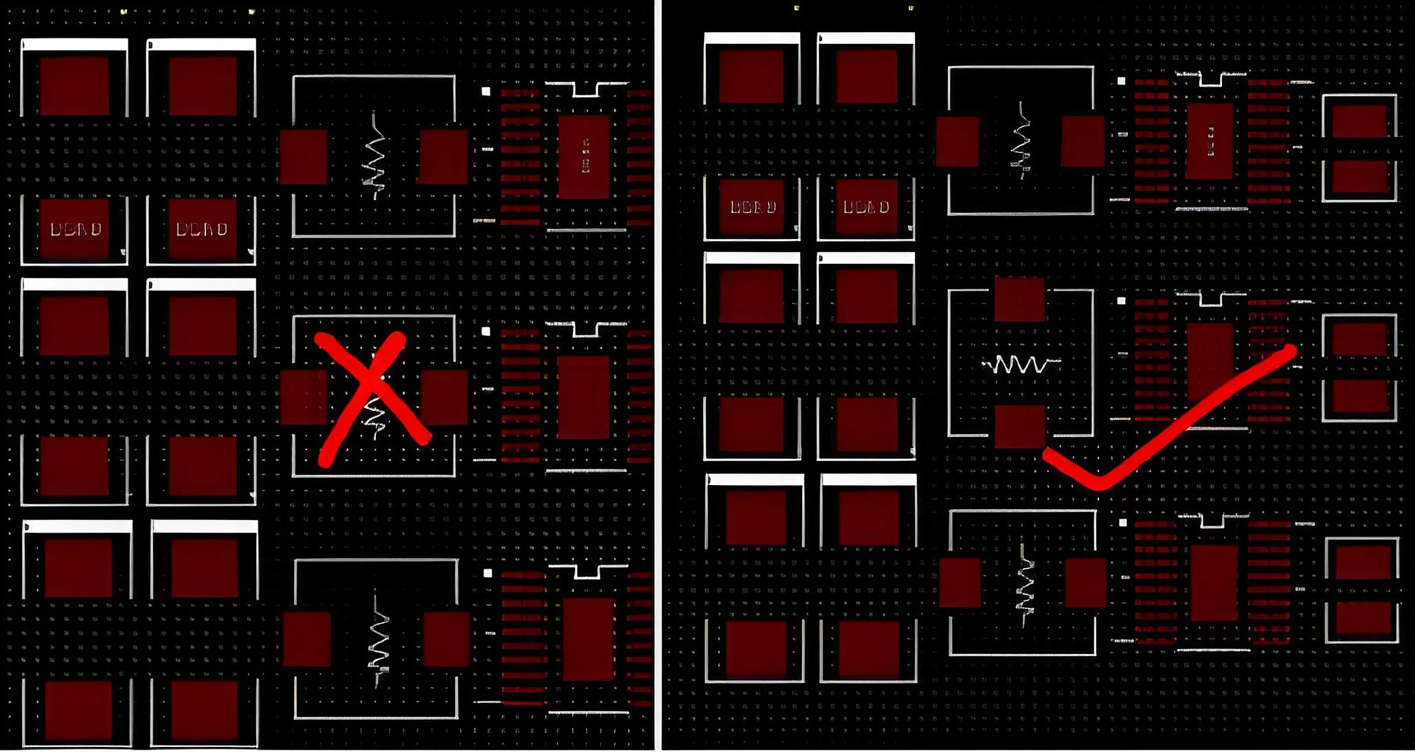
Improper Component Placement
Irregular and incorrect component arrangement may cause signal interference, temperature problems, and assembly difficulties. Designers should carefully arrange all PCB components in the correct order.
Insufficient Trace Routing
Adjust the trace width according to the current carrying capacity to avoid overheating and voltage drop issues.
Inaccurate Solder Pad Size
Improper solder pad size design may affect component soldering and mechanical stability.
Improper Power and Ground Line Design
If the power and ground lines are designed too thin or improperly laid out, it will cause uneven power distribution and affect circuit stability.
Neglecting Thermal Management
For components with higher power, if heat dissipation is not fully considered, it may lead to overheating, shortening the lifespan of components or even causing damage.
Incorrect Component Package Selection
Choosing inappropriate component packages may lead to unstable connections, difficulty in routing, or failure to meet heat dissipation requirements.
Confusion Between Signal Pins and Power Pins
Incorrect identification of signal pins and power pins may lead to wiring errors.
Unreasonable PCB Stacking
Unreasonable layering or incorrect number of layers may lead to signal crosstalk and electromagnetic interference issues.
Component Layout Remaining
During layout, test points should be reserved for subsequent circuit debugging and fault analysis.
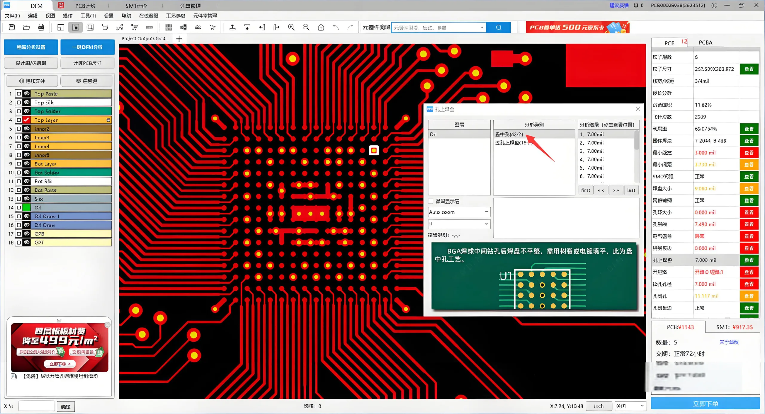
Lack of DFM (Design for Manufacturing) Optimization
Consider manufacturing feasibility during design to avoid limitations on minimum trace width and via size.
Conclusion
High-power PCB design is a systematic project that requires comprehensive consideration of multiple aspects such as thermal management, electrical performance, and mechanical structure. Through the above design ideas and techniques, newcomers to high-power PCB design can better grasp the design direction, avoid common traps, and gradually improve their design capabilities. Remember, practice is the sole criterion for testing truth, and continuous accumulation of experience will make you more proficient in the field of high-power PCB design.

Superb post however , I was wanting to know if you could write a litte more on this subject? I’d be very grateful if you could elaborate a little bit further.