PCB: The Heartbeat of Modern Electronics

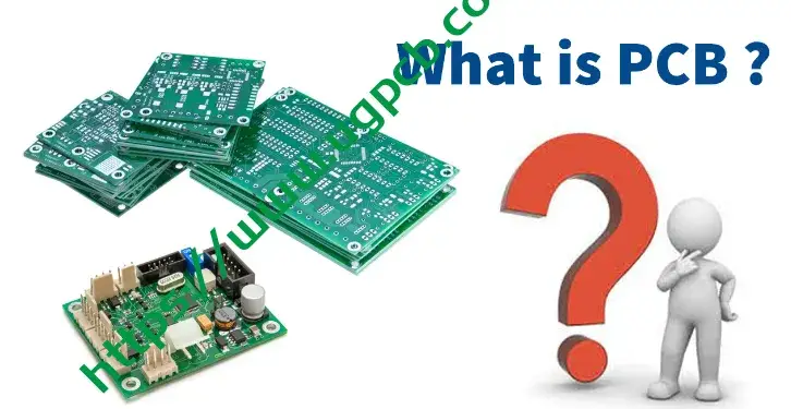
PCB, short for Printed Circuit Board, serves as the backbone of modern electronic devices. Constructed from a base substrate, insulation materials, and copper foil, PCBs utilize printing and etching processes to create circuits. Alternatively known as PWB (Printed Wire Board) in the United States and Britain, these boards are crucial for supporting and connecting various electronic components.
The Role of PCB
PCBs are vital electronic components that not only support electronic assemblies within a PCBA board but also provide circuit connections for various electronic parts. By connecting capacitors, resistors, inductors, IC chips, and other necessary components, PCBs function as the motherboard or mainboard of electronic devices.
Almost every electronic gadget, from headphones and batteries to computers, communication equipment, airplanes, satellites, automobiles, ships, and medical devices, relies on PCBs. PCBA, which stands for Printed Circuit Board Assembly, refers to a PCB populated with various electronic components.
The Origin of PCB
The history of PCBs dates back to 1925 when Charles Ducas, the pioneer of the additive process, successfully created conductors for wiring by printing circuit patterns on an insulating substrate and using electroplating. In 1936, Paul Eisler, the pioneer of the subtractive process, first used PCBs in radios.
The application of PCB technology in military radios began in 1943, and by 1948, the United States officially approved PCBs for commercial use. In the 1950s, with the resolution of bonding strength and solderability issues of CCL and laminated boards, the copper etching method became mainstream, and PCBs began to be widely used. Since then, PCBs have dominated the electronics industry.
Evolution of PCB Technology
From single-sided PCBs in the 1950s to double-sided and then multi-layer PCBs in the following decades, the industry has witnessed significant advancements. The 1970s saw rapid developments in multi-layer PCBs, moving towards high precision, high density, fine lines, small holes, high reliability, low cost, and automated continuous production.
In the 1980s, Surface Mount Technology (SMT) gradually replaced through-hole mounting, and ultra-high multi-layer PCBs and High-Density Interconnect (HDI) boards flourished. By the 1990s, packaging technology evolved from Quad Flat Packages (QFP) to Ball Grid Arrays (BGA), prompting PCBs to develop smaller circuits.
Into the 21st century, high-density BGA, chip-scale packaging, and organic laminate materials for IC packaging substrates have seen rapid growth in PCB technology. PCBs have evolved from single-layer to double-layer, multi-layer, flexible, rigid-flexible combinations, metal-based, ceramic, and more, each maintaining its unique development trend.
The Functions of PCB
Before PCBs, electronic components were interconnected through wires. PCBs provide mechanical support for fixing and assembling integrated circuits and other electronic components, enabling wiring and power connections (signal transmission) or electrical insulation among them. They also offer required electrical properties such as characteristic impedance.
Adopting PCBs in electronic devices avoids the errors associated with manual wiring, facilitates automatic component insertion or mounting, soldering, and testing, ensuring product quality, enhancing productivity, reducing costs, and simplifying maintenance. PCBs simplify assembly and soldering, reduce traditional wiring workloads, and lighten labor intensity.
Classifications of PCB
By Application
- Consumer PCBs: Used in toys, cameras, televisions, audio equipment, mobile phones, lights, home appliances, etc.
- Industrial PCBs: Used in security, automobiles, computers, communication devices, instruments, industrial controllers, etc.
- Military PCBs: Used in aerospace, radar, military ships, and military communication equipment.
By Base Material
- Paper-based PCBs: Phenolic paper-based and epoxy paper-based.
- Glass cloth-based PCBs: Epoxy glass cloth-based and Teflon glass cloth-based.
- Synthetic fiber PCBs: Epoxy synthetic fiber-based.
- Organic film-based PCBs: Nylon film-based.
- Ceramic substrate PCBs.
- Metal core-based PCBs: Iron, aluminum, copper.
- Hydrocarbon compound PCBs.
- Ceramic powder PCBs.
- PTFE, Teflon PCBs.
By Structure
- Rigid PCBs
- Flexible PCBs
- Rigid-flexible combination PCBs
By Layer Count
- Single-sided PCBs: One-layer boards with components and markings on one side and circuitry on the other.
- Double-sided PCBs: Circuits on both sides connected through vias.
- Multi-layer PCBs: Containing internal circuit layers, typically 4 to 20 layers.
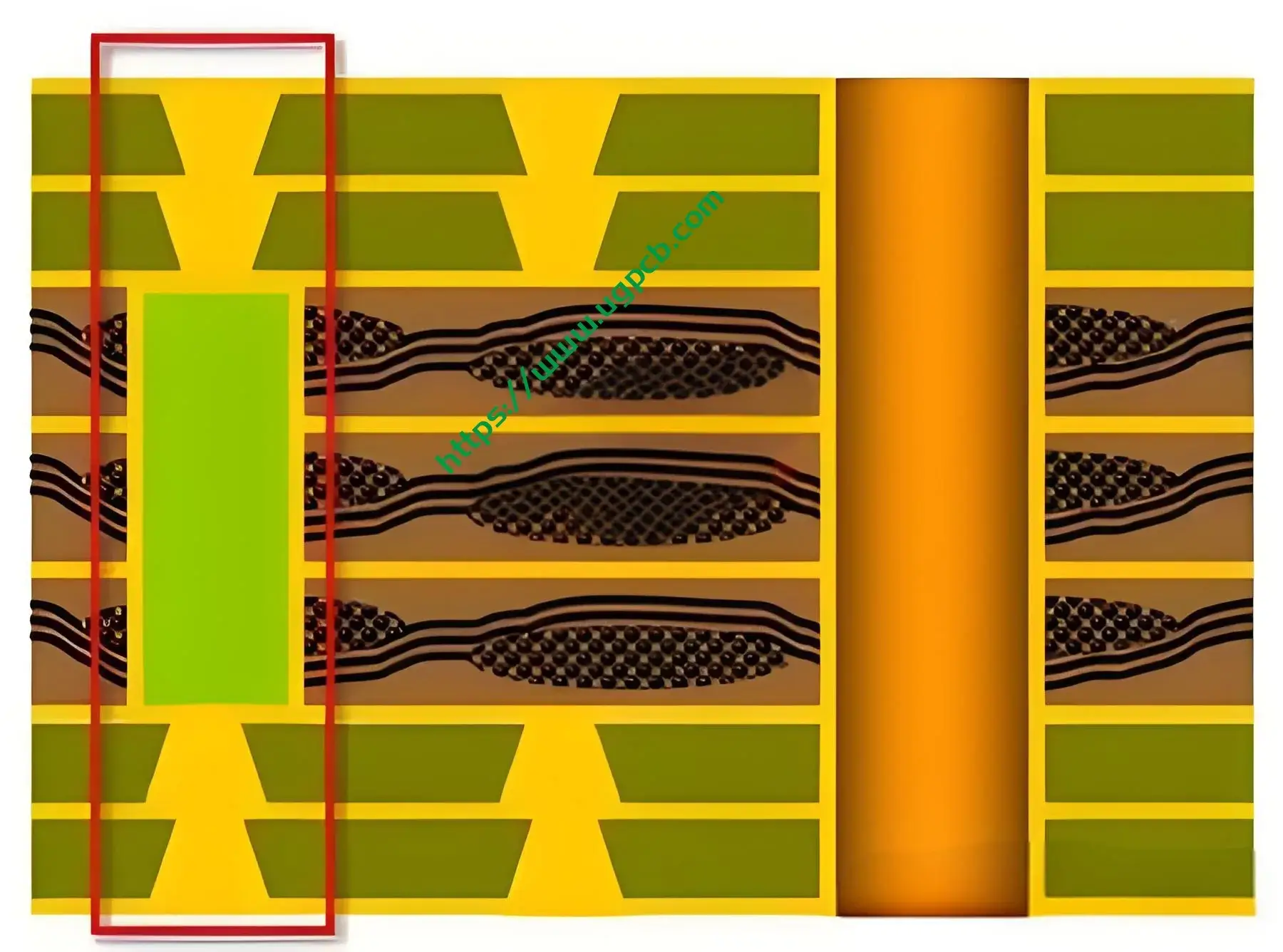
- HDI PCBs: High-density interconnect boards with micro vias and buried vias, commonly used in mobile phone motherboards.
The Structure of PCB
PCBs consist of Copper Clad Laminates (CCL), Prepreg (PP sheets), copper foil, solder mask (also known as solder resist), and silkscreen layers. Surface treatments protect the exposed copper foil from oxidation and ensure effective soldering.

CCL (Copper Clad Laminates)
CCL, or copper-clad laminate, is a composite material made by bonding glass fiber cloth and copper foil with epoxy resin as a binder. CCL is the basic material for manufacturing PCBs, providing conductivity, insulation, and support. The performance, quality, and manufacturing cost of PCBs largely depend on CCL.
Prepreg (PP Sheets)
Prepreg, also known as PP sheets, is one of the main materials used in the production of multi-layer PCBs. It consists of resin and reinforcing materials such as glass fiber cloth. Prepreg softens under heat and pressure and solidifies upon cooling.
Copper Foil – Circuit Layer
Copper foil, a thin, continuous metal foil deposited on the PCB substrate, serves as the conductor. It adheres to the insulating layer and is etched to form circuit patterns. Common copper foil types include rolled copper foil (RA) and electrolytic copper foil (ED).
Solder Mask
The solder mask, usually green but also available in red, black, and blue, is a permanent protective layer on the PCB, preventing moisture, corrosion, mold, and mechanical damage. It also prevents components from being soldered incorrectly.
Silkscreen Layer
The silkscreen layer, typically located above the solder mask, provides annotations and labels such as component values, outlines, manufacturer logos, and production dates, aiding in PCBA installation and maintenance.
PCB Surface Treatment
Surface treatment refers to coating the connection points on PCBs, such as pads or contact points, with a protective layer. Common surface treatments include lead tin plating, lead-free tin plating, Organic Solderability Preservatives (OSP), Electroless Nickel/Immersion Gold (ENIG), immersion silver, immersion tin, and gold finger plating. With tightening environmental regulations, lead tin plating has been phased out, and most PCBs now comply with RoHS and halogen-free manufacturing processes.
Conclusion
PCBs are indispensable components in modern electronics, facilitating error-free wiring, automated assembly, and cost-effective production. As technology evolves, PCBs continue to adapt, ensuring they remain a cornerstone of electronic innovation.
 UGPCB LOGO

