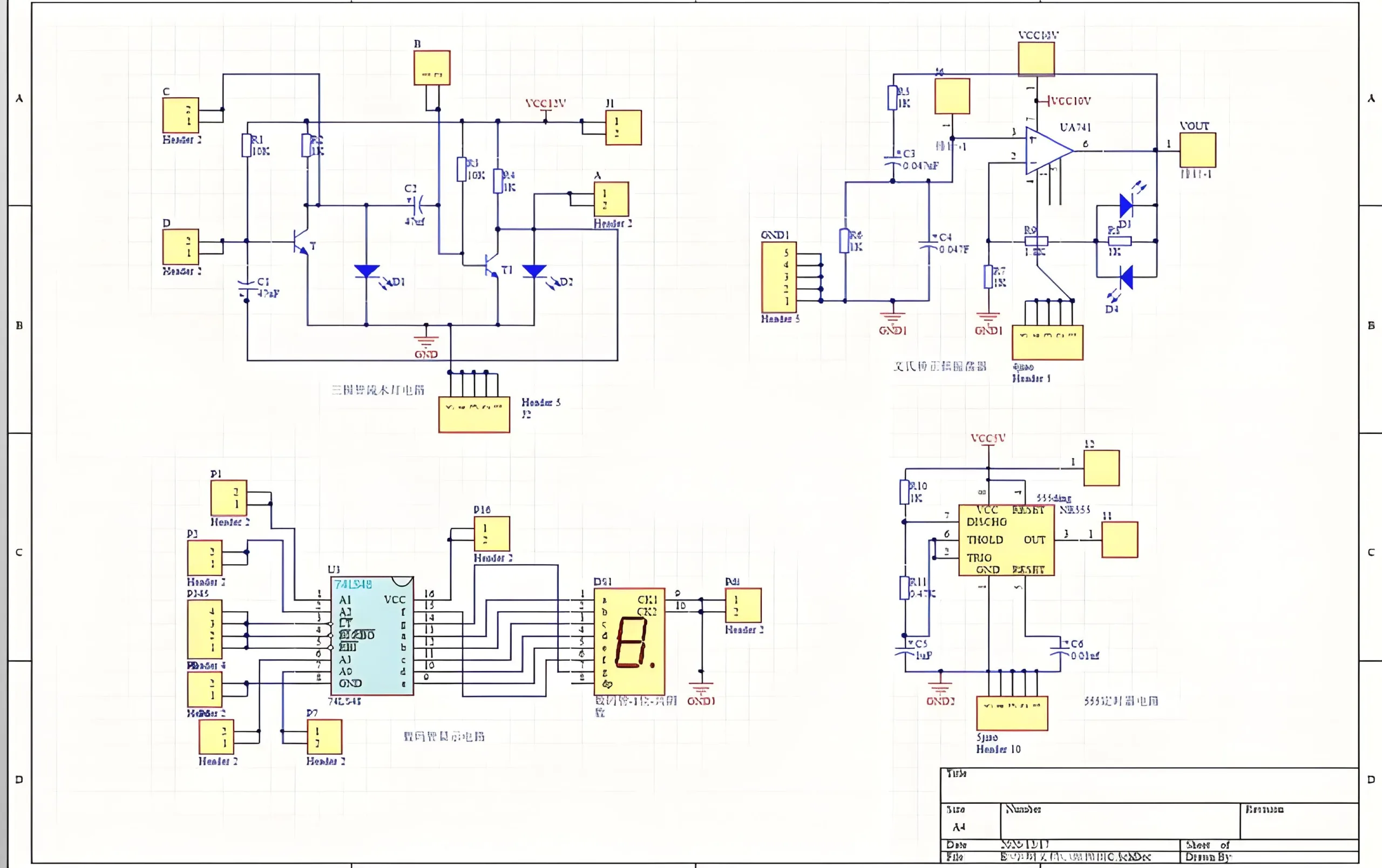
PCB schematic directly displays the structure and working principle of electronic circuits,so it is generally used in the design and analysis of circuits. When analyzing the circuit, we can understand the basic working principle of the circuit by identifying various circuit component symbols drawn on the circuit diagram and the connection mode between them.Circuit board diagram is a tool used to reflect the working principle of an electronic circuit.
Do a test, function test, and maintenance in the electronics industry.Suppose you can understand the PCB diagram of the product. In that case,you will get twice the result with half the effort, and the testability will be significantly improved,which can improve the production efficiency and delivery quality of the product.At present,it is mainly divided into digital circuits and analog circuits. The digital circuit is relatively simple,and the analog circuit is rather difficult to understand and has a wide range.

PCB schematic
PCB diagram includes circuits with the following modules so that the circuit sub-module analysis will be more precise. The main modules are:
1.Power supply circuit. For each circuit to work typically, there must be a regular power supply, so almost every course has a power supply circuit.
2.The control circuit is generally a digital circuit. Action and control include MCU, FPGA, CPLD, DSP, etc. It is usually composed of digital circuits.
3.Signal circuit and general control circuit are control signal circuits that provide corresponding signals and measure corresponding signals.Therefore,signal circuits are generally analog circuits with driving circuits. Or relay circuit.
4.Communication circuit, theoretically speaking,is a part of the control circuit. Because these have some particular communication protocols, they are specially listed,which are generally digital circuits.
5.Storage circuit is the storage function of some data.It is generally divided into serial and parallel.Now there are SPI,IIC,and other memory.
6.Interface circuit, some input and output interface circuits, such as protective circuit,external connector circuit,etc.
The PCB schematic of the product is divided into several parts, and the approximate position of each piece is analyzed carefully by the module circuit. This will be much simpler than the whole circuit board diagram.
PCB board diagram design software
From Protel to Altium
As long as you are engaged in electronics, you know Protel, just like you know the windows operating system as long as you use a computer because many of its operating habits have been rooted in the hearts of electronic people. Protel is a CAD software for the circuit industry launched by the port company (now Altium company) in the late 1980s.It is well deserved to be in front of many EDA software and is the preferred software for circuit designers.
From the original PCB design tool in the DOS environment to the now powerful Altium Designer,Altium has launched many different versions.As far as I know,there are many versions used as follows:
Protel99SE:although it is a very early version,many companies are still using it.We are using it.Even some companies only recognize this version of documents.
Protel2004sp4:in 2002, Altium released PrtelDXP.In addition to some enthusiasts who started to try early, some people still hold Protel99SE, and some even now. However, there are still many new functions that attract new users after all.When they have to change the version, many people may directly use the latest version of protel2004. In addition, the later version is no longer named after Protel, so many people take this version as a Pretel Memorial.When opening new types of files that Protel99SE cannot open, All use this second stage classic version.
Altium designer 6.8: in 2005, Altium officially released Altium designer 6.0.Since then,the era of Protel has ended. Until 2007, Altium designer 6.8 was released, which is the latest version at present.I believe many people haven’t used it very much, but many people should try it first. It is said that the software integrates all the technologies and functions required for the integrated development of electronic products.It provides a unified application for electronic engineers and designers. It includes board system design, FPGA level system design, embedded software development based on FPGA and discrete processors,PCB layout, editing, and manufacturing.And integrated into the modern design data management function. Previously released tools such as P-CAD were gradually integrated into Altium designer after 2006. However, I don’t particularly agree with this approach. Circuit design mainly uses circuit board diagram and PCB design.
Orcad and cadence
OrCAD is an EDA software launched by OrCAD company in the late 1980s. Many people are not unfamiliar with it. It is known as the best tool for drawing circuit board diagrams.
However, there is better news,that is,later, cadence acquired OrCAD, and then Orcad and Allego can also carry out the interactive design. Therefore, many people use OrCAD (later called design entry cis) for the schematic design and Allego for PCB layout design to achieve the best partner.

Cadence Allegro PCB Design Software
Of course,Orcad and Allego are not brothers after all. There may be a running-in period if they can be the best partners. Moreover, OrCAD also has the original brother PCB tool orcadrayout. Allego also has the original sibling diagram design tool designentryhdl. Some people even use OrCAD to draw schematic diagrams, generate network tables,and then use pretel to draw PCBs. In order to take into account the usage habits of many people, cadence has integrated all tools (excluding pretel) into an integrated environment.Users can use whatever they want.
Today, cadence calls these tools cadence allegro system interconnection design platform,which mainly includes:designentrycis (OrCAD) schematic design tool, designentryhdl schematic design tool,allegropc editor printed circuit board design tool (Allegro for short), allegroams simulator simulation tool Allegropcbsi signal integrity analysis tool, etc. It is worth mentioning that cadence has done better in high-speed signal simulation.As we all know,with the increasing signal frequency and smaller volume of circuit board cards, not all circuit boards can work normally if they are connected correctly. Therefore, signal integrity analysis is becoming more and more necessary.Cadence provides many such tools,such as constraint manager in PCBedit, which can help users consider the integrity of signals to a great extent.
Cadence not only provides CadenceAllegro system interconnection design platform,but also provides IC design tools, and IC design will be a compulsory lesson for electronics engineers in the near future. Just as PCB boards are very common now, IC will be common in the future. For example,there are SMIC companies in the Chinese mainland that can undertake such projects, but for ordinary users, It may only take a period of time.
PADS/PowerPCB
Although padpower appeared late and was not understood by the majority of users, it may be accepted by the majority of electronic circuit designers because it not only continues the characteristics of “powerful function and simple operation” of pads but also has great improvement. It may be because it is closely related to PCB manufacturing. It has gradually become popular since powerpcb5.0. Therefore, many people know about PowerPCB. I think it can be understood that the names of pads and PowerPCB are somewhat inconsistent in different versions.
The original pads series includes PowerLogic (PowerPCB(PCB tool), HyperLynx (signal analysis tool), and other main tools. At present, the latest version pads2007, which is widely used, includes main tools such as dxdesigner (Project Management), padlogic, pad layout (PCB tool), HyperLynx (signal analysis tool). Up to now, pads have indeed become a fully functional and powerful EDA software, whether from PCB schematic design, PCB design, high-speed signal analysis, or overall project management.
 UGPCB LOGO

WeChat
Scan the QR Code with WeChat