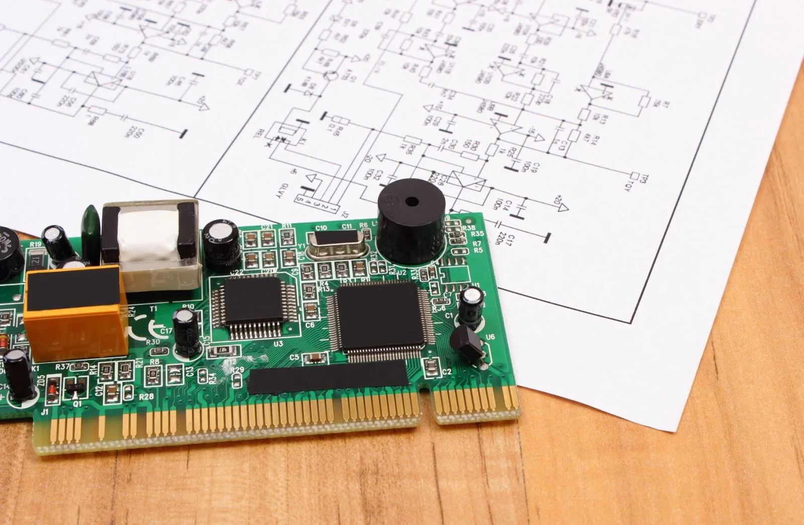
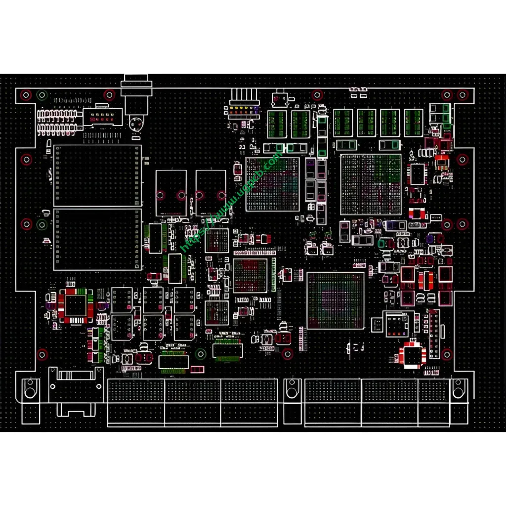
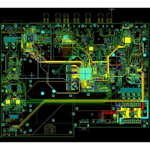
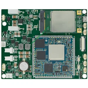
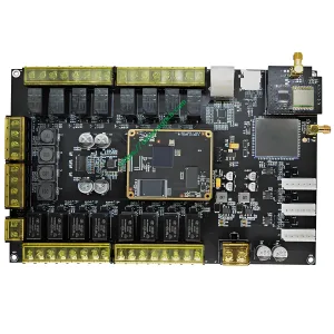
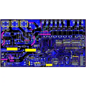
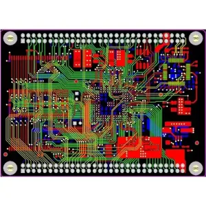
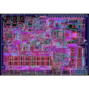
The optoelectronic printed circuit board is a new generation of packaging substrate with high computing requirements that collects light and transmits electrical-to-optical signals and uses electricity for computing.
The optoelectronic circuit board according to the present invention is an optoelectronic circuit board in which at least a rigid portion formed and laminated with a conductor circuit and an insulating layer and one or more bendable flexible portions are integrated, an external connection portion for mounting An optical element and/or a package substrate on which the optical element is mounted is formed in the above-mentioned rigid portion, and an optical path is formed in at least one of the above-mentioned flexible portions.
 UGPCB LOGO
