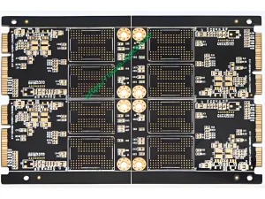
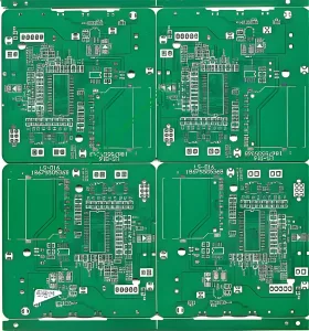
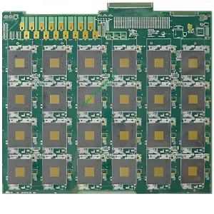
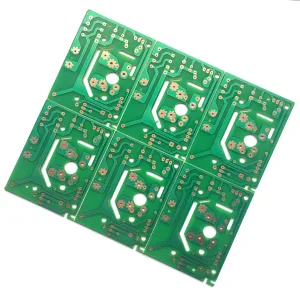
Introduction to PCB Board Bonding
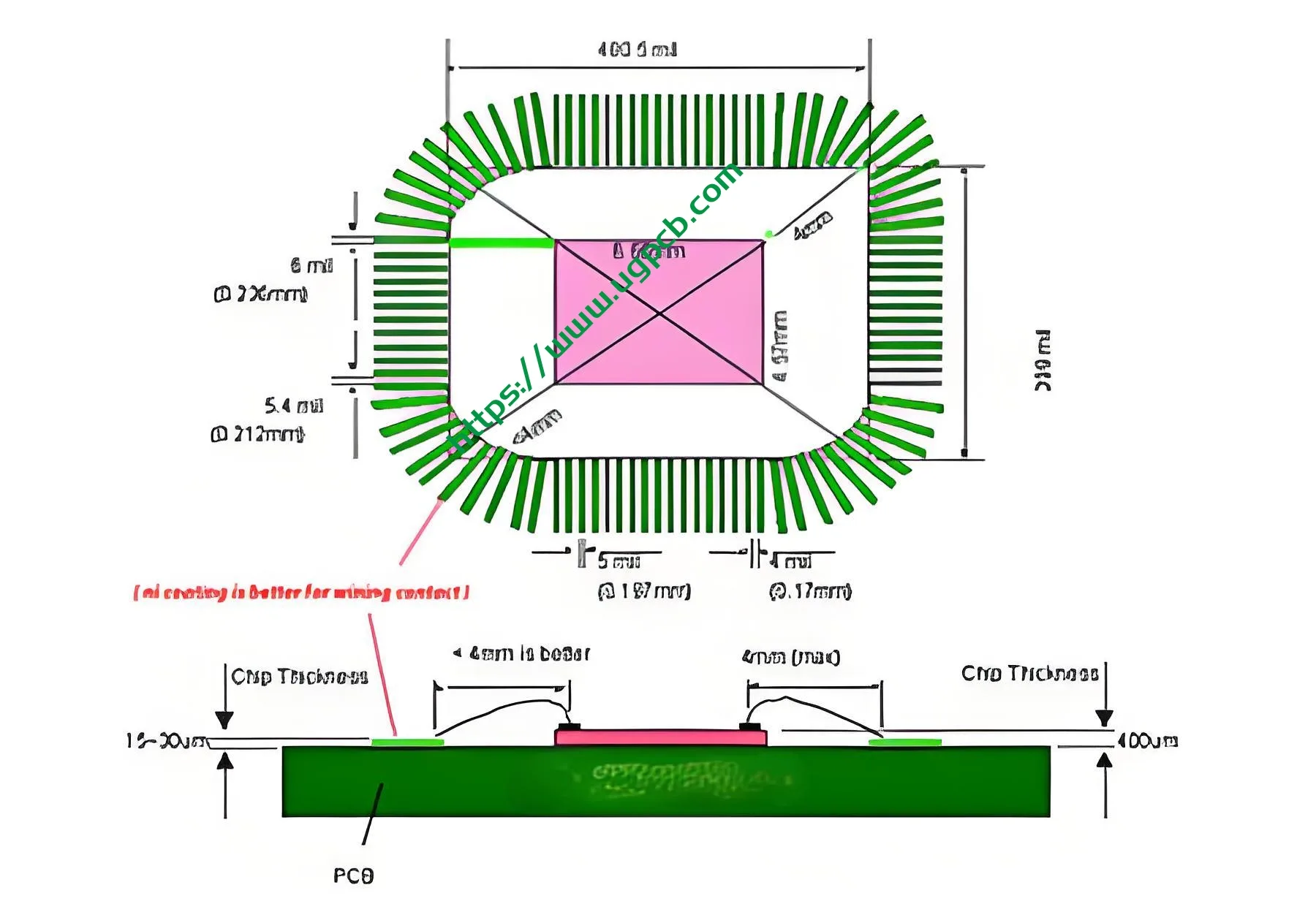
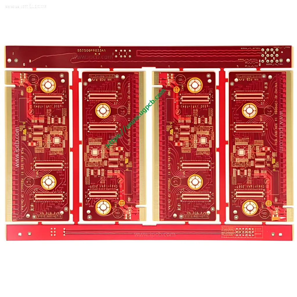
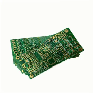
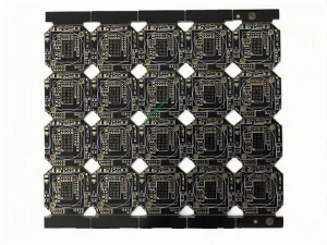
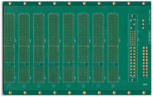
PCB Board bonding is a wiring method in the chip production process. It typically connects the gold or aluminum wire of the chip’s internal circuit with the package pin or gold-plated copper foil of the circuit board before packaging. The ultrasonic wave from the generator (usually 40-140kHz) generates high-frequency vibration transmitted to the cleaver through the horn. When the cleaver touches the lead wire and weldment, under pressure and vibration, the metal surfaces rub against each other, destroying the oxide film and causing plastic deformation. This results in close contact between two pure metal surfaces, achieving atomic-distance combination and forming a firm mechanical connection. Post-bonding, the chip is usually packaged with black glue.
PCB Bonding Method Overview
This section discusses the PCB bonding method and its process requirements.
Process Flow
The process flow for PCB bonding includes:
-
Cleaning PCB
- Wipe oil, dust, and oxide layers from the bond location with a cloth.
- Clean the test position with a brush or air gun.
-
Dropping Adhesive
- Use a moderate amount of glue.
- Place four glue points evenly at the corners.
- Ensure the bonding glue does not contaminate the pad.
-
Chip Bonding
- Use a vacuum suction pen with a flat suction nozzle to avoid scratching the wafer surface.
- Check the chip direction.
- Bond the chip to the PCB “stably and straightly”: flat, parallel, and tightly attached without virtual positioning; stable, not easy to fall off during the process; correctly aligned with the reserved position on the PCB.
-
Bonding Standards
- The PCB must pass the Bondin pull test with specified wire strengths.
- Standard aluminum wire with a bonding melting point has specified tail dimensions.
- The aluminum wire solder joint should be oval, with specified length and width.
- Operators should handle wires carefully, align points accurately, and observe the bonding process under a microscope for defects.
-
Sealing with Glue
- Before sealing, check the plastic ring’s regularity and ensure it is centered and not distorted.
- Install the plastic ring close to the wafer surface without occluding the photosensitive area.
- The black glue should cover the aluminum wire and bonding chip, not exposing the wire or sealing out the PCB sun circle.
- Control the drying temperature and time strictly.
- Ensure no air holes on the black glue surface, and the height should not exceed the plastic ring.
-
Testing
- Combine various test methods: manual visual inspection, automatic welding line quality inspection, and automatic optical image analysis (AOI) with X-ray analysis to check inner solder joint quality.
 UGPCB LOGO

