UG,PCB, PCBA and PECVD customization, prototyping and manufacturing producer

Download | About | Contact | Sitemap

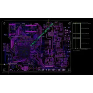
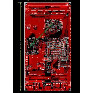
RF Printed Circuit Board Design - UG

RF PCB Design/

RF Printed Circuit Board Design

Name: RF Printed Circuit Board Design

Designable layers: 1-32 layers

Minimum line width and line spacing: 3mil

Minimum laser aperture: 4mil

Minimum mechanical aperture: 8mil

Copper foil thickness: 18-175цm (standard: 18цm35цm70цm)

Peel strength: 1.25N/mm

Minimum punching hole diameter: single side: 0.9mm/35mil

Minimum hole diameter: 0.25mm/10mil

Aperture tolerance: ≤φ0.8mm±0.05mm

Hole tolerance: ±0.05mm

  • Product Details

Definition of RF PCB

We can generally define an RF PCB as a printed circuit board designed to operate at medium to very high frequencies.

Frequency Range of RF PCBs

Therefore, any high frequency printed circuit board that operates above 100MHz is a radio frequency printed circuit board (UGPCB).

Actual Reference Frequency Range

However, when it comes to RF PCBs (UGPCB), the actual reference frequency range is usually 300MHz and above.

Microwave PCBs

RF PCBs operating above 2GHz are called microwave PCBs.

Prev:

Next:

Leave a Reply

Leave a message