
The Essential Role of PCBs in Electronics
In the realm of electronics manufacturing, Placas de circuito impresso (PCB) serve as a vital core component. Acting like the nerve center of electronic devices, they connect various components, ensuring seamless electricity and information flow. But have you ever pondered why the thickness of the copper layer on these PCBs is expressed in ounces? This article delves into this intriguing detail, exploring the science and art behind determining PCB copper layer thickness.
Why Copper Thickness Matters
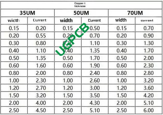
Consider the high-tech gadgets like smartphones or laptops; each houses one or more PCBs. A critical aspect of these boards is the thickness of their copper foil, impacting not just conductivity and heat dissipation but also the product’s durability and cost. The choice of expressing copper thickness in ounces over length units simplifies calculations related to density and conductivity, making design and manufacturing more straightforward. Ounces offer a direct correlation with conductivity—more weight means better conductivity due to a higher number of copper atoms.
Standardizing Thickness for Universality
The standardization of using the ounce unit in PCB manufacturing fosters clear communication and collaboration among designers and manufacturers, avoiding confusion across diverse materials and processes.
Standard PCB Copper Layer Thicknesses
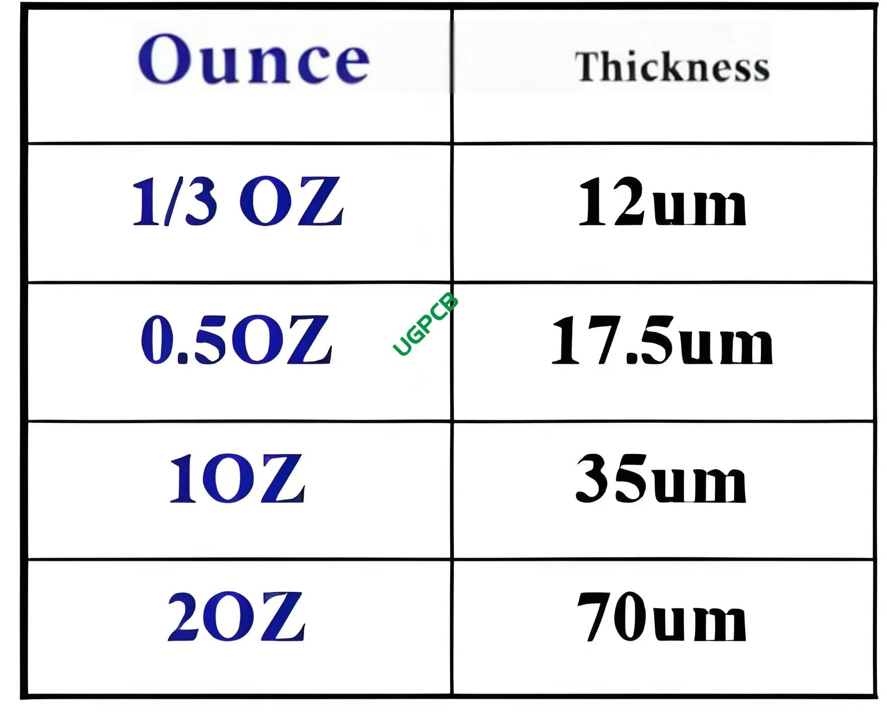
Standard PCB copper thicknesses are categorized into several specifications, incluindo 1 ounce (aproximadamente 35 microns), 2 ounces (sobre 70 microns), e 3 ounces (around 105 microns). These standards cater to different application needs:
- Single-sided and double-sided PCBs typically use a 1-ounce copper layer.
- Multi-layer boards feature inner layers with 1/2 ou 1/3 ounce copper, while outer layers may vary between 1, 1/2, ou 1/3 ounce.
- Special applications requiring higher current capacities might necessitate up to 2 ou 3 ounces per square foot.
Balancing Thickness for Performance and Cost
While thicker copper layers enhance conductivity and heat dissipation, they also increase weight, custo, and manufacturing complexity. Por isso, selecting the appropriate thickness involves a balance between application-specific requirements and cost considerations.
Impact on Circuit Performance
Copper layer thickness directly influences a circuit’s conductivity and heat dissipation efficiency, crucial for stable and reliable electronic equipment operation. Adequate copper thickness bolsters the PCB’s mechanical strength and longevity, particularly in challenging environments.
Embracing Technological Advancements
As technology progresses and electronic devices become more sophisticated, so do the demands on PCBs. Future advancements will likely lead to smaller, more efficient devices, with green manufacturing and recyclability gaining prominence. In this landscape, mastering the nuances of PCB copper layer thickness selection becomes increasingly important for industry practitioners and enthusiasts.
Conclusão: A Crucial Link in Electronics Progress
Understanding and innovating within the realm of PCB copper layer thickness is integral to advancing electronics manufacturing. By grasping the underlying principles and continuously exploring new frontiers, we contribute to the evolution of electronic equipment, pushing the boundaries of what’s possible in this dynamic field.
