e,PCB, Personalização de PCBA e PECVD, produtor de prototipagem e fabricação

Download | Sobre | Contato | Mapa do site

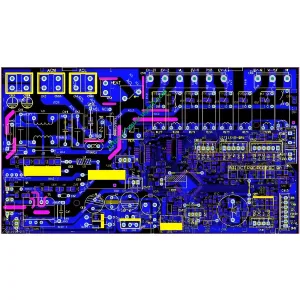
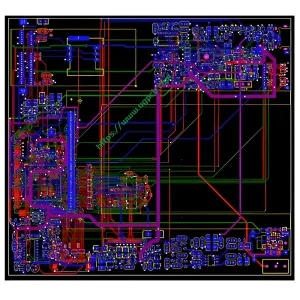
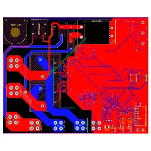
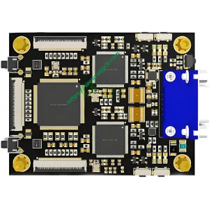
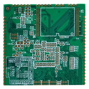
10-layer communication switch PCB/PCBA design - e

Design de PCB multicamadas/

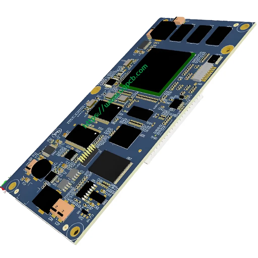
10-layer communication switch PCB/PCBA design

Nome: 10-layer communication switch PCB/PCBA design

Folha: IT180, F4BM, FR4, FR1-4, etc..

Designable layers: 1-32 camadas

Minimum line width and line spacing: 3mil

Minimum laser aperture: 4mil

Minimum mechanical aperture: 8mil

Copper foil thickness: 18-175цm (standard: 18цm35цm70цm)

Força de casca: 1.25N/mm

Minimum punching hole diameter: single side: 0.9mm/35mil

Minimum hole diameter: 0.25mm/10mil

Aperture tolerance: ≤φ0.8mm±0.05mm

  • Detalhes do produto

What is a Communication Switch?

What is a communication switch?

Switched Communication Network

A switched communication network transfers data from a source to a destination through a series of network nodes.

Adaptive Communication Switch

Purpose and Functionality

Adaptive switches allow users with physical difficulties and special needs to activate assistive technology devices in their environment.

Importance of the Right Switch

Deceptively simple buttons, the right switch will open up access to a world of communications equipment, environmental controls, computer software, and mobile devices.

Anterior:

Próximo:

Deixe uma resposta

Deixe um recado