
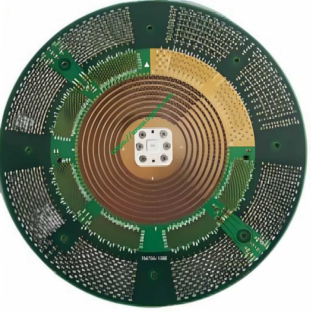
Introduction to the 44-Layer IC Probe Card PCB
The 44-Layer IC Probe Card PCB is a high-performance, multilayered printed circuit board designed for testing integrated circuit (CI) chips. This sophisticated product ensures accurate and reliable testing of semiconductor devices, making it an essential tool in the manufacturing and quality assurance processes of the electronics industry.
What is a 44-Layer IC Probe Card PCB?
A 44-Layer IC Probe Card PCB is a specialized type of PCB used for interfacing with integrated circuit chips during their testing phase. It features 44 layers of conductive material, which provide ample pathways for electrical signals to travel, ensuring comprehensive testing coverage.
Como funciona?
The probe card works by establishing physical and electrical contact with the microscopic pads on the IC chip. Each layer of the PCB is meticulously designed to align with specific test points on the chip, allowing for precise measurement of electrical parameters such as voltage, current, and resistance.
Aplicações e propósito
Primarily, these probe cards are utilized in the semiconductor industry to test the functionality and performance of IC chips before they are packaged and soldered into electronic devices. They help in identifying any defects or malfunctions, ensuring only high-quality chips reach the market.
Types of IC Test PCBs
There are generally two main types of IC test PCBs:
- Probe Cards: Used for testing unpackaged chips directly from the wafer.
- Load Boards: Employed for testing packaged chips, often with more stringent impedance requirements due to higher speed interfaces.
Composição de materiais
The 44-Layer IC Probe Card PCB is made from TUC/TU872HF material, known for its excellent electrical properties and durability. The choice of material ensures that the PCB can withstand the rigorous demands of semiconductor testing.
Características de desempenho
With a structure comprising 10mil, 12mil, and 14mil layers, this PCB offers enhanced signal integrity and reduced interference. The surface technology includes hard gold plating ranging from 3 para 15 microns, which provides superior conductivity and corrosion resistance. Special processes like metal cladding and depth control drilling further enhance its performance and reliability.
Características estruturais
The PCB’s design includes varying layer thicknesses to accommodate different testing needs, with L1-L44 at 10mil, L1-L28 at 12mil, and L29-L44 at 14mil. This intricate layering allows for detailed and accurate testing of complex IC chips.
Processo de Produção
The manufacturing process of a 44-Layer IC Probe Card PCB involves several critical steps:
- Projeto: Using specialized software to create the layout and ensure all test points are accurately placed.
- Seleção de material: Choosing high-quality materials like TUC/TU872HF for optimal performance.
- Camadas: Empilhar várias camadas de material condutor para formar a estrutura da PCB.
- Perfuração: Creating holes for through-hole components and vias using depth control drilling techniques.
- Revestimento: Applying hard gold plating to ensure excellent conductivity and durability.
- Conjunto: Componentes e conectores de montagem no PCB.
- Teste: Conducting thorough tests to verify the PCB’s functionality and reliability.
Use cenários de caso
These probe cards are predominantly used in:
- Semiconductor Fabs: For in-house testing of new IC designs.
- Quality Assurance Labs: To ensure compliance with industry standards.
- Centros de pesquisa e desenvolvimento: For experimenting with new semiconductor technologies.
Para concluir, the 44-Layer IC Probe Card PCB is an indispensable tool in the semiconductor industry, providing precise and reliable testing for IC chips. Seu design avançado, materiais de alta qualidade, and rigorous production process make it a preferred choice for ensuring the highest standards of quality and performance in electronic devices.


