1. Micro-wiring technology realizes 30um/30um Line/Space
2. The small-diameter VIA technology of laser forming realizes high-density wiring
3. Use thermosetting synthetic resin with excellent reliability
4. The corresponding surface treatment (Ni/Au, SAC Soldering, etc.) can be implemented according to the packaging requirements
5. Green products such as lead-free and fluorine-free can be provided
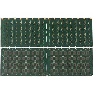
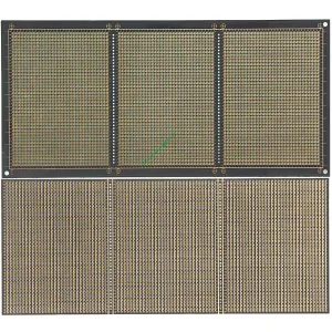
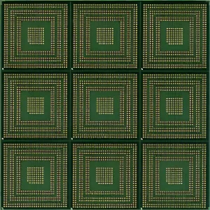
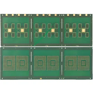
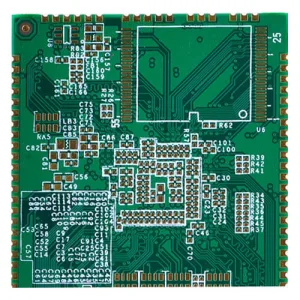
With the vigorous development of new ICs such as BGA (Array da grade de bola) and CSP (Chip Scale Packaging), IC substrates have been booming, and these ICs need new packaging carriers. As one of the most advanced PCBs (Placas de circuito impresso), the IC substrate PCB, together with any layer HDI PCB and flexible rigid PCB, has explosive growth in popularity and application, and is now widely used in telecommunications and electronic updates.
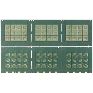
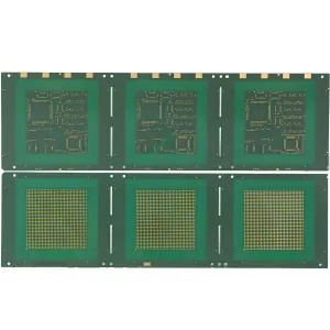
An IC substrate is a substrate used to package bare IC (Circuito integrado) chips. Connecting chips and circuit boards, IC is an intermediate product with the following functions:
• It captures semiconductor IC chips;
• Internal wiring to connect the chip and PCB;
• It can protect, strengthen and support IC chips and provide heat dissipation tunnels.
IC substrate classification
um. Classified by package type
• BGA IC substrate. This IC substrate performs well in terms of heat dissipation and electrical performance, and can significantly increase chip pins. Portanto, it is suitable for IC packages with more than 300 pinos.
• CSP IC substrate. CSP is a single chip package, light weight, tamanho pequeno, and similar size to IC. CSP IC substrates are mainly used in memory products, telecommunications products and electronic products with a small number of pins.
•FC IC substrate. FC (flip chip) is a package that flips the chip, with low signal interference, low circuit loss, good performance and effective heat dissipation.
•MCM IC substrate. MCM is an abbreviation of multi-chip module. This type of IC substrate absorbs chips with different functions into one package. Portanto, due to its characteristics including lightness, thinness, shortness and miniaturization, this product can be the best solution. Claro, since multiple chips are packaged in one package, this type of substrate does not perform well in terms of signal interference, dissipação de calor, and fine wiring.
b. Classified by material properties
• Rigid IC substrate. It is mainly made of epoxy resin, BT resin or ABF resin. Its CTE (Coeficiente de Expansão Térmica) é sobre 13 para 17 ppm/°C. •Flex IC substrate. It is mainly made of PI or PE resin and has a CTE of 13 to 27ppm/°C•ceramic IC substrate. It is mainly made of ceramic materials, such as aluminum oxide, aluminum nitride or silicon carbide. It has a relatively low CTE, sobre 6 to 8ppm/°C
c. Classification by bonding technology
• Wire bonding
•TAB (automatic keyboard keying)
•FC bonding
Application of IC substrate PCB
IC substrate PCB is mainly used in light-weight, light-weight and powerful electronic products, such as smart phones, notebook computers, tablet computers and networks, como telecomunicações, medical treatment, controle industrial, aerospace and military fields.
Rigid PCB passes through multi-layer PCB, traditional HDI PCB, SLP (substrate-like PCB) to a series of innovative substrate PCBs of IC. SLP is just a rigid PCB, and its manufacturing process is similar to a semiconductor scale.
Difficulties in manufacturing IC substrate PCB
Compared with standard PCBs, IC substrates must overcome the difficulties of high performance and advanced functions in manufacturing.
The IC substrate is thin and easily deformed, especially when the thickness of the board is less than 0.2 milímetros. To overcome this difficulty, breakthroughs must be made in board shrinkage, lamination parameters and layer positioning systems to effectively control substrate warpage and lamination thickness.
 LOGOTIPO UGPCB





I went over this web site and I conceive you have a lot of superb info , bookmarked (:.