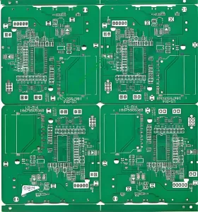
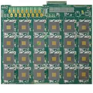
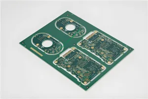
Introduction to the 18Layers Communication Base Station PCB
The 18Layers Communication Base Station PCB is a high-performance printed circuit board designed specifically for telecommunication applications. It offers exceptional signal integrity and reliability, making it ideal for complex communication systems that require precise data transmission and minimal interference.
Purpose and Applications
This sophisticated PCB is primarily used in base station equipment for telecommunication networks. It supports various functions such as signal processing, data routing, and connectivity, ensuring smooth operation of communication systems. The product is crucial in enhancing network performance and coverage.
Classification and Specifications
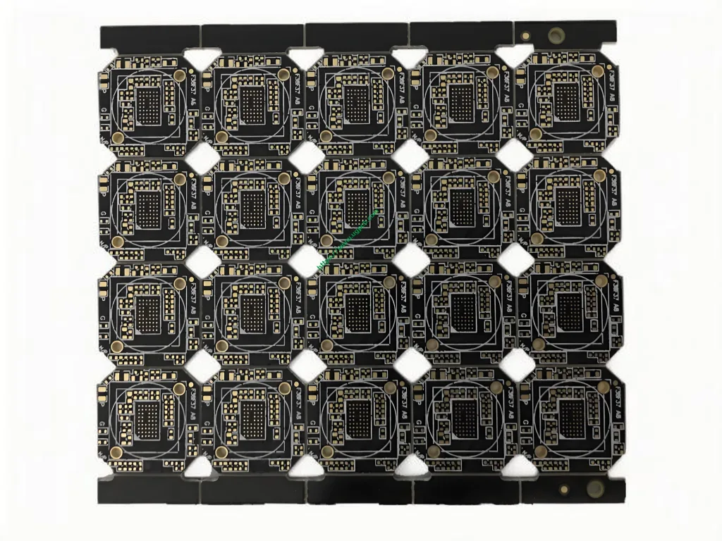
The Surveillance Camera PCB Board falls under the category of high-density interconnect (IDH) PCB. It features six layers and is constructed from SY S1000-2 TG170 FR4 material, which provides excellent thermal stability and mechanical strength. The copper thickness is 1OZ, and the finished thickness is 1.2mm, optimized for durability and performance.
Composição de materiais
Crafted from SY S1000-2 TG170 FR4, this PCB material ensures high glass transition temperatures, low dielectric constant, and stable electrical properties. It is ideal for applications requiring superior signal integrity and resistance to environmental stressors.
Performance and Features
The PCB boasts an immersion gold surface treatment that enhances its corrosion resistance and solderability. With a trace/space of 3mil/3mil (0.075MM/0.075MM) and a minimum hole size of 0.2mm (8mil), it supports fine-pitch components and intricate designs. Special processes like blind and buried vias are employed to increase the board’s density without compromising its functionality.
Projeto Estrutural
The layer structure of 1-2,5-6,7-12 allows for efficient routing of signals and power, minimizing crosstalk and electromagnetic interference. This design is critical for maintaining signal clarity and overall system performance in high-speed communication base stations.
Processo de Produção
The manufacturing process involves several stages, including drilling, plating, gravura, and final inspection. Each step is meticulously executed to ensure the highest quality standards. Advanced technologies such as laser drilling and precision etching are utilized to achieve the desired specifications.
Usage Scenarios
This PCB is commonly used in telecommunication base stations where reliable and high-speed data transmission is paramount. It is also suitable for other applications requiring robust and high-performance PCB solutions, such as advanced surveillance systems and industrial control equipment.
Conclusão
Resumindo, the 18Layers Communication Base Station PCB is a state-of-the-art solution tailored for demanding telecommunication environments. Its advanced materials, precise manufacturing processes, and innovative design make it a reliable choice for enhancing network performance and efficiency.
 LOGOTIPO UGPCB

