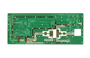
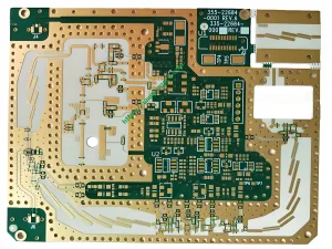
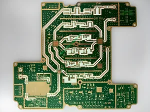
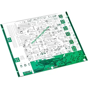
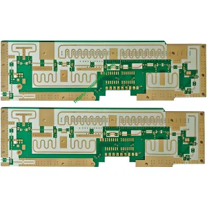
Overview of Teflon PCB
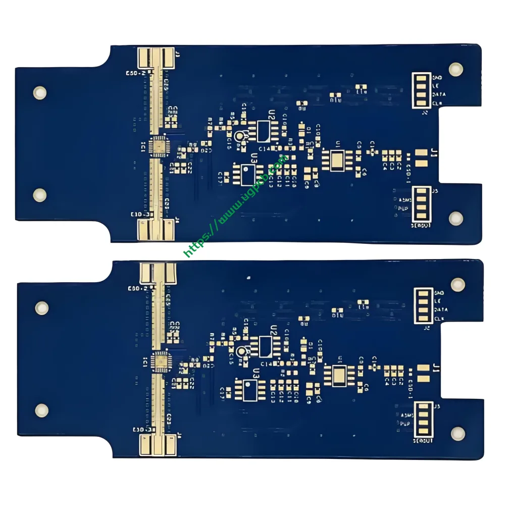
PCB de teflon, known for its exceptional performance in high-frequency applications, is a type of printed circuit board (PCB) that utilizes Teflon laminate material. This material is chosen for its superior dielectric properties, making it ideal for microwave and high-frequency electronic devices. The quality of Teflon PCBs typically adheres to the IPC6012 Class II or Class III standards, ensuring reliable and consistent performance.
Definition and Key Specifications
A Teflon PCB is defined by its use of Teflon as the dielectric material, which offers a dielectric constant ranging from 2.0 para 3.5. These boards can be manufactured with a layer count ranging from 2 para 34 camadas, providing flexibility for various complexities in circuit design. The thickness of Teflon PCBs can vary from 0.1mm to 12mm, catering to different application needs. The copper thickness usually starts with a base of 0.5oz and can be finished up to 1oz, ensuring adequate conductivity for high-frequency signals.
Design Considerations
When designing Teflon PCBs, several key factors need to be considered:
- Constante dielétrica (Dk) and Dissipation Factor (Df): Materials must have precise Dk and Df values to ensure signal integrity and minimize loss at high frequencies.
- Layer Count and Thickness: Depending on the complexity of the circuit, the number of layers and overall thickness can be adjusted within the specified ranges.
- Espessura do Cobre: Adequate copper thickness is crucial for maintaining low impedance and reducing signal loss.
- Surface Technology: Options like Immersion Gold and ISIG (Immersion Silver) are available for surface finishes, each offering different benefits in terms of conductivity and reliability.
Princípio de funcionamento
Teflon PCBs operate based on the principle of controlled impedance and minimal signal loss, which is essential for high-frequency applications. The Teflon material’s low dielectric constant helps in maintaining signal integrity by reducing phase delays and attenuation. This makes Teflon PCBs particularly suitable for microwave and RF (Radiofrequência) applications where signal purity is critical.
Aplicações
The primary application of Teflon PCBs is in the field of microwave and high-frequency electronics. They are used in devices such as radar systems, satellite communications, and other RF components where high performance and reliability are paramount. The ability to handle high frequencies with minimal loss makes Teflon PCBs an excellent choice for these demanding applications.
Classificação
Teflon PCBs can be classified based on their layer count, grossura, and specific applications. Common classifications include:
- Single-Sided and Double-Sided Boards: For simpler applications with fewer layers.
- Multilayer Boards: For more complex circuits requiring multiple layers of interconnections.
- High-Frequency Specific Boards: Designed specifically for microwave and RF applications, often with stringent requirements on material properties and manufacturing precision.
Material Properties
The unique properties of Teflon make it an ideal material for high-frequency PCBs:
- Low Dielectric Constant: Helps in reducing signal delay and loss.
- Stable Performance Across Temperature Ranges: Ensures consistent performance in varying environmental conditions.
- High Resistance to Moisture Absorption: Prevents degradation of signal quality due to moisture ingress.
Processo de Produção
The production of Teflon PCBs involves several steps:
- Seleção de material: Choosing the appropriate Teflon material based on the required Dk and Df values.
- Circuit Design: Creating the circuit layout with considerations for high-frequency performance.
- Gravura: Removing unnecessary copper to create the desired circuit pattern.
- Laminação: Bonding multiple layers together under high pressure and temperature.
- Surface Finishing: Applying the chosen surface technology, such as Immersion Gold or ISIG.
- Testing and Quality Control: Ensuring the final product meets all specifications and standards.
Use cenários
Teflon PCBs are used in scenarios where high-frequency performance is critical, como:
- Microwave Antennas: For efficient signal transmission and reception.
- Satellite Communications: Ensuring reliable data transfer between Earth and space.
- Radar Systems: Providing accurate and stable signal processing capabilities.
Para concluir, Teflon PCBs are specialized circuit boards designed for high-frequency applications, offering excellent dielectric properties and signal integrity. Their design, materials, and production processes are tailored to meet the stringent requirements of microwave and RF technologies.
 LOGOTIPO UGPCB

