In the process of PCBA surface mount assembly, various electronic components often fail. Astăzi, we share a case study on the failure analysis of a 3A linear regulator, explaining how to look beyond the surface and quickly identify the fault.
1) Chip failure description: Vin is short-circuited to ground.
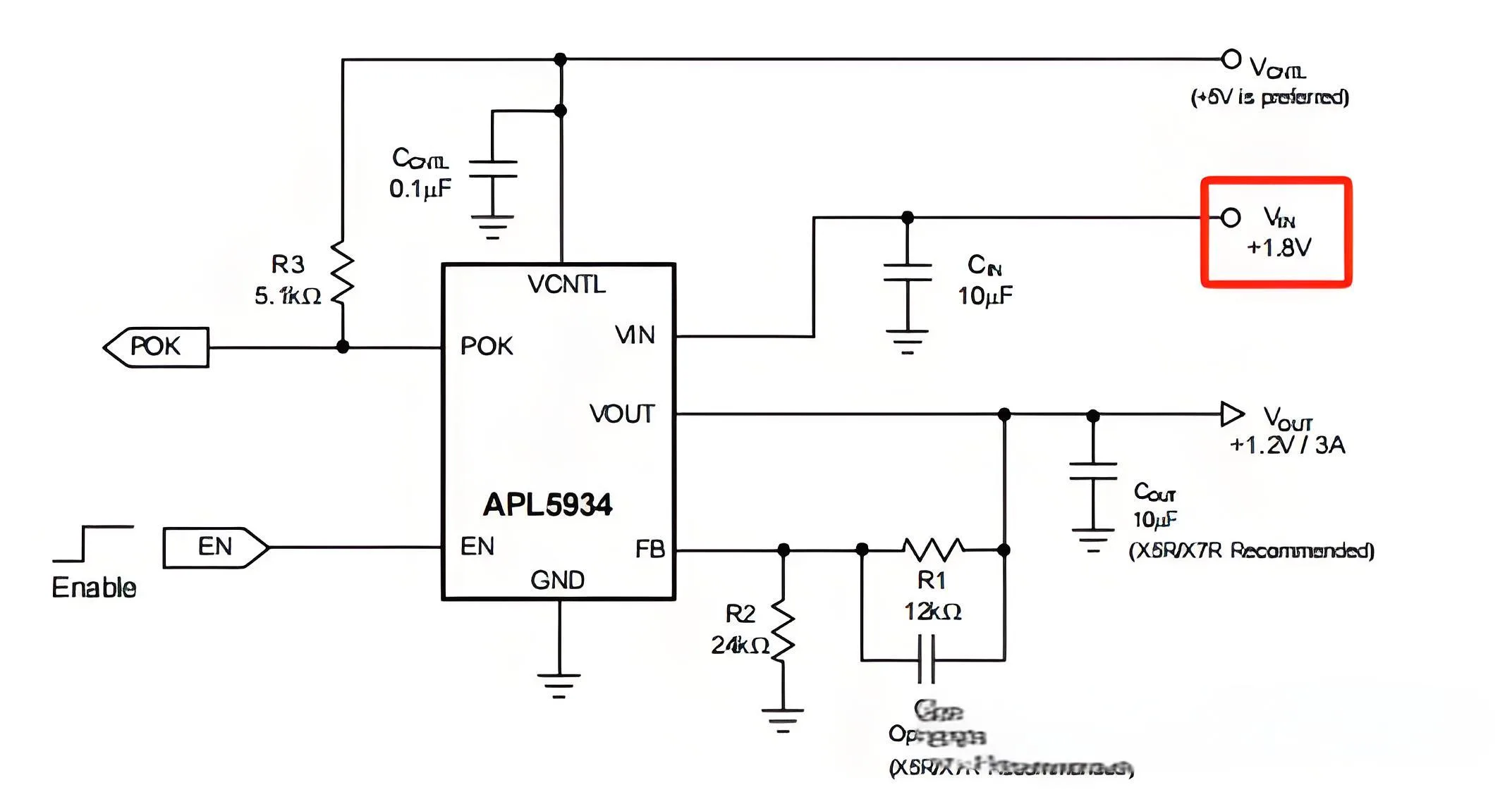
Vin is short-circuited to ground.
2) Device failure analysis: The chip experienced an EOS (Electrical Over-Stress) failure as confirmed by IV testing with Vin short-circuited to ground.
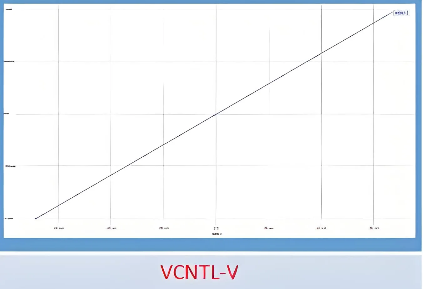
IV test confirms Vin to ground short circuit.
No obvious anomalies were observed in appearance or acoustic scanning, but X-ray revealed suspected burn damage.
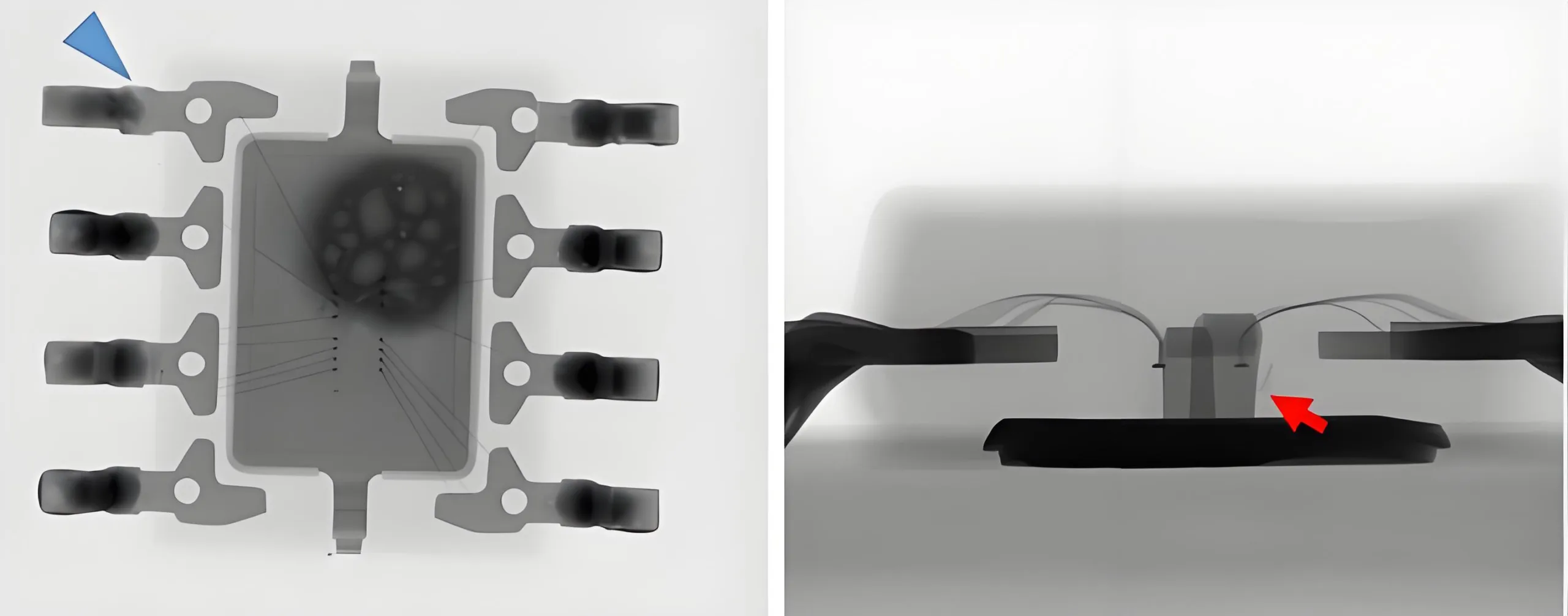
Suspected to have been burned
Upon opening the cover, it was found that the chip’s EOS burnout was most severe at the VCNTL pin rather than Vin.
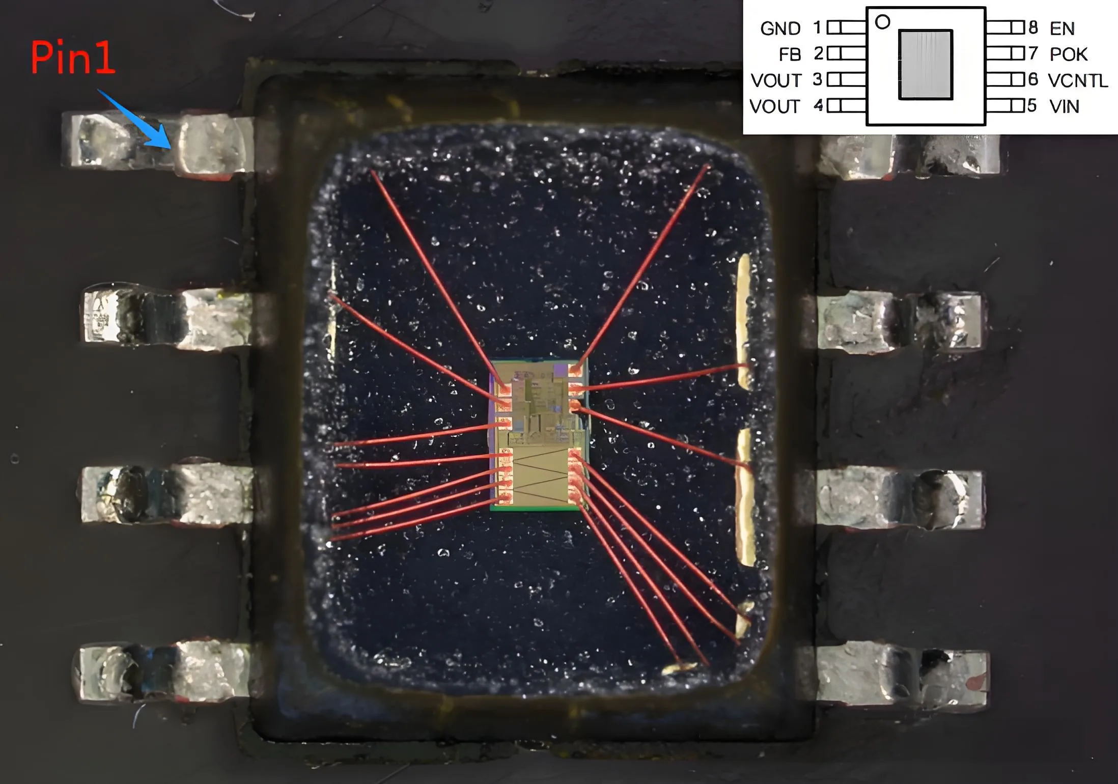
The chip’s EOS has been burned out
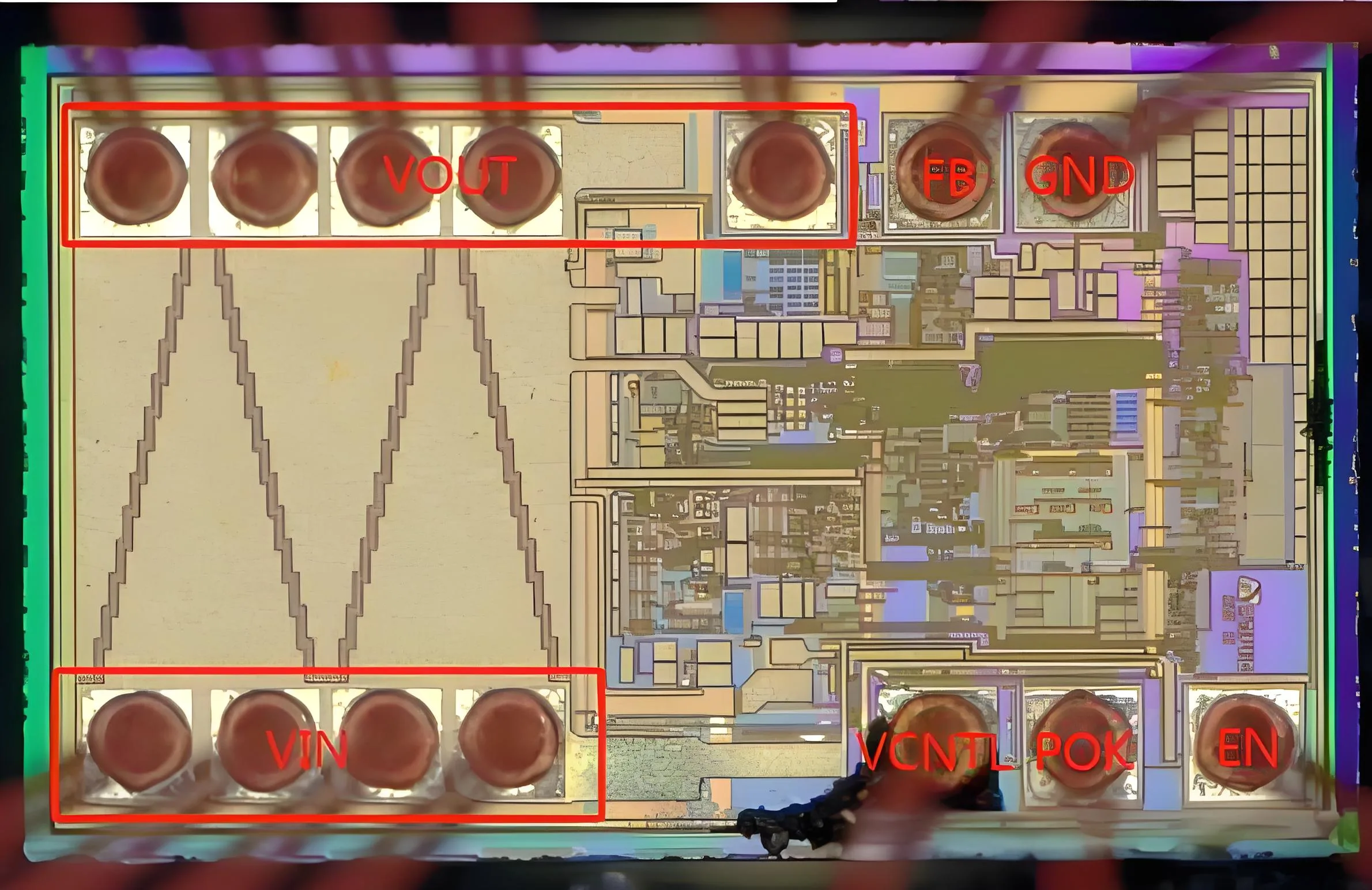
The chip’s EOS has been burned out
3) Root cause analysis: It is suspected that over-voltage stress introduced by VCNTL caused the chip failure. The VCNTL pin is defined as an input pin, which could potentially experience over-voltage stress.
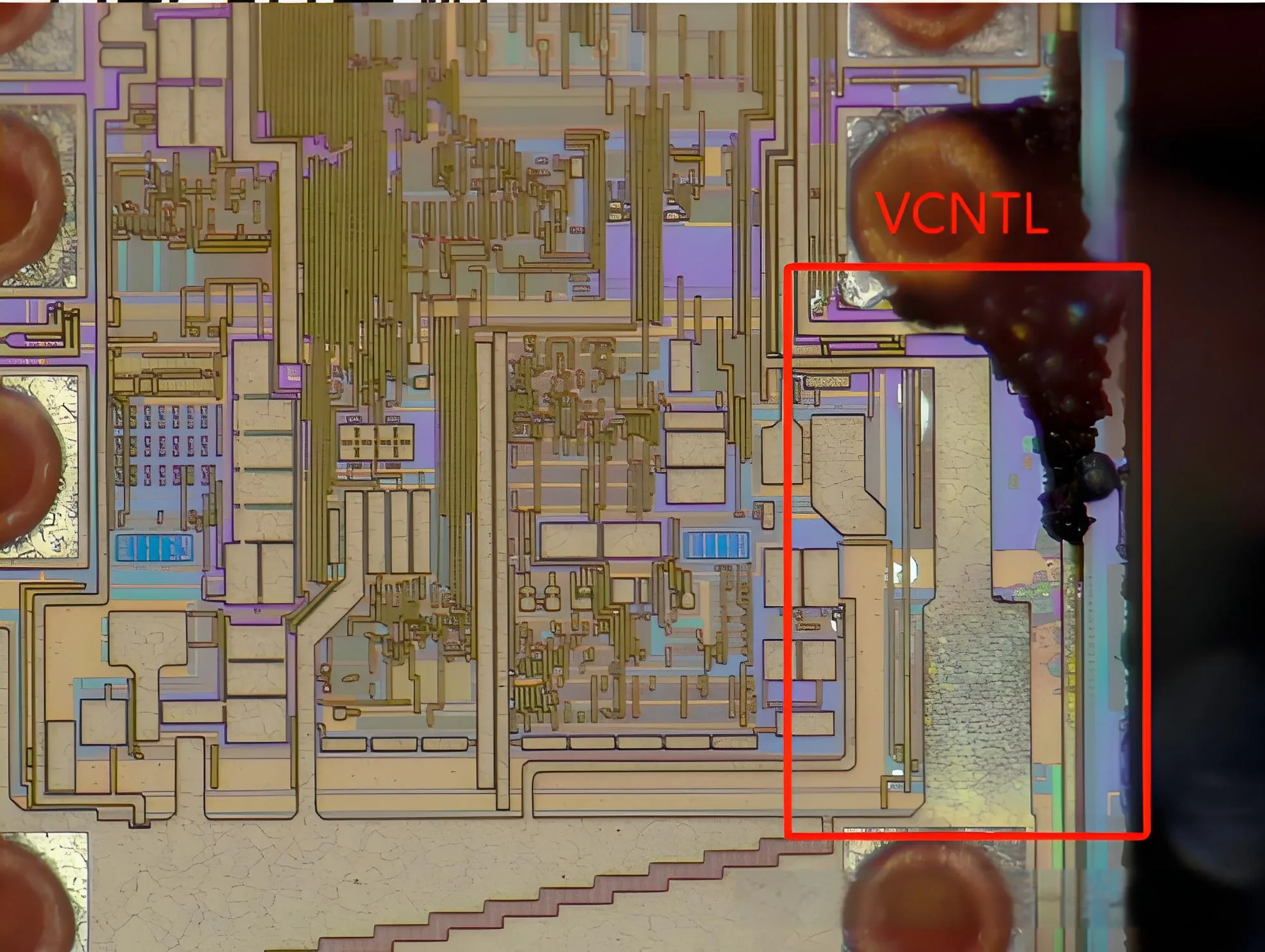
VCNTL introduces excessive electrical stress leading to failure
Further analysis revealed that the metal morphology along the VCNTL-VIN link appeared melted, and measuring the IV between VCNTL and VIN showed a short circuit. Prin urmare, the chip failed due to over-voltage stress introduced by VCNTL. Analysis of the chip’s logic block diagram matched the failure phenomenon with its logical function.
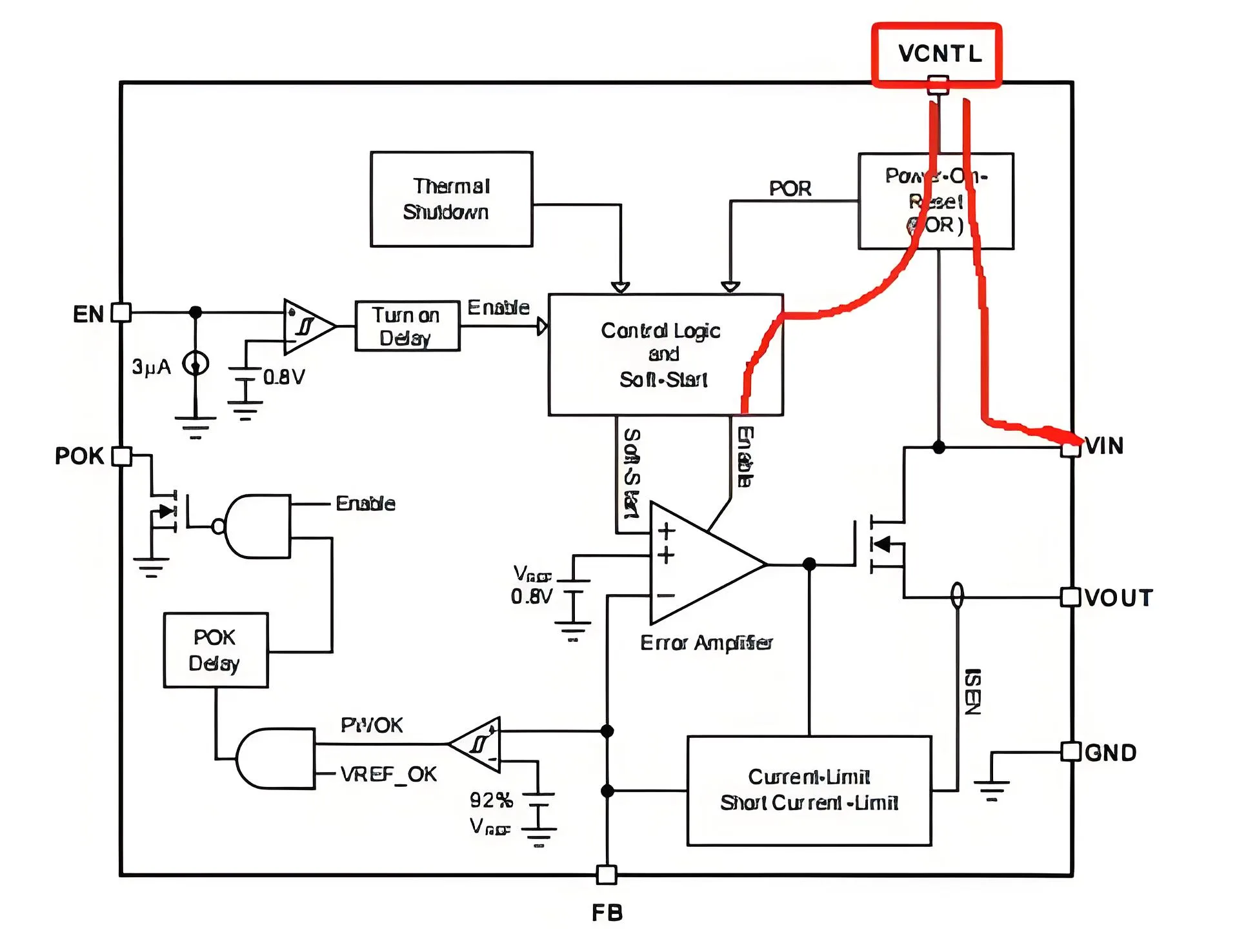
Chip Logic Diagram
Removing the top layer of metal clarified that the chip’s failure was indeed caused by over-voltage stress introduced by VCNTL.
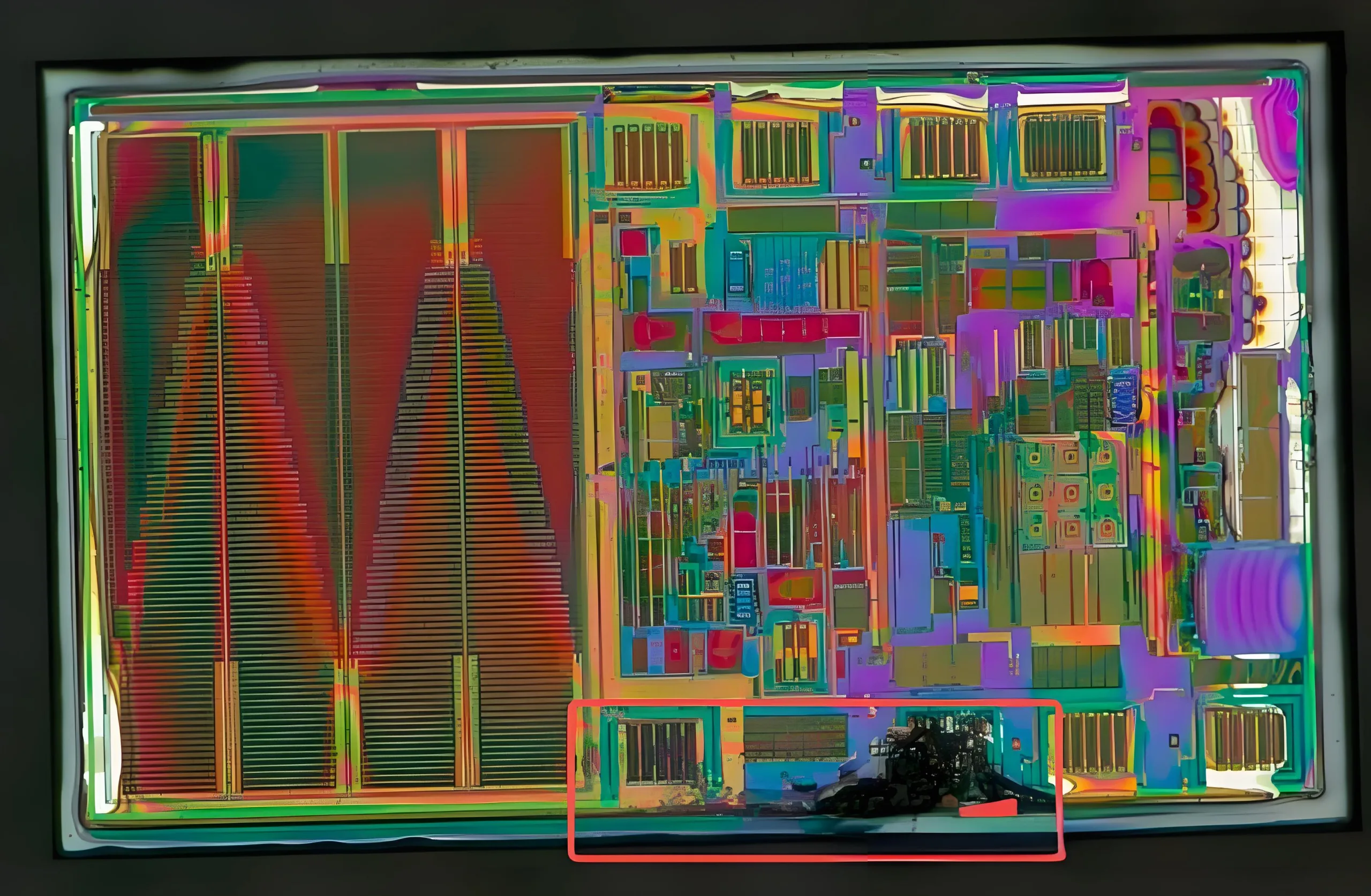
VCNTL introduces excessive electrical stress leading to failure.
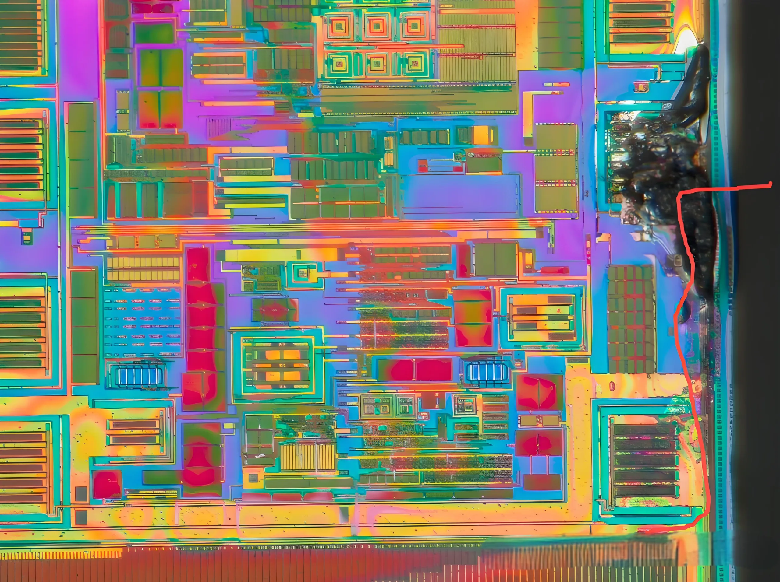
VCNTL introduces excessive electrical stress leading to failure.
4) Board level confirmation: After analysis, it was confirmed that damage to other peripheral devices on the board caused the voltage stress on the VCNTL pin to exceed its specification value. De aici, this chip was a “victim.”
EOS is the most common phenomenon encountered in failure analysis. Identifying the root cause through EOS failure symptoms is challenging and requires analysts to have clear logical thinking and extensive knowledge.
 LOGO UGPCB

