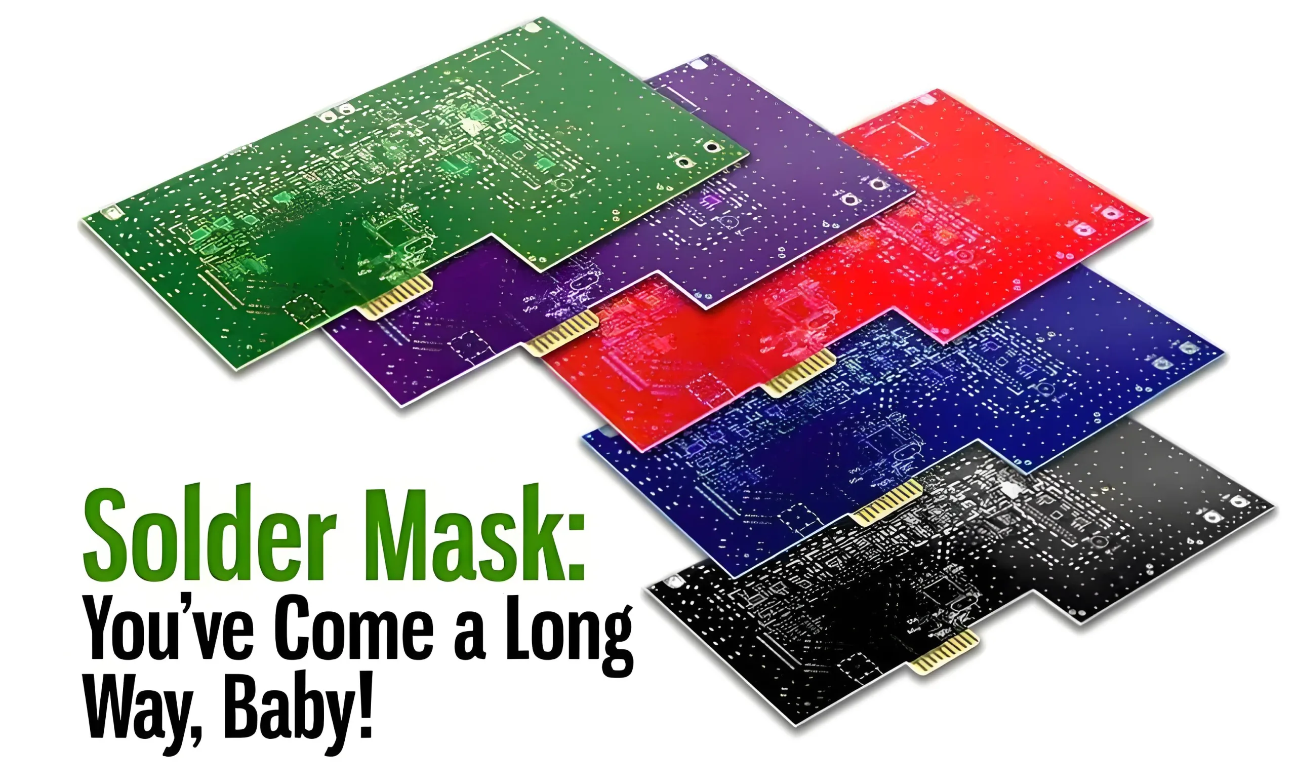
In the world of electronics, full of creativity and challenges, PCB (Placă de circuit tipărită) undoubtedly serves as the heart of hardware products, while solder mask design adds a beautiful touch to its surface. Astăzi, let’s delve into the world of PCB solder mask design, exploring everything from color selection and solder mask bridge design to the discussion of four major coverage processes, revealing the ingenuity behind every detail.

PCB solder mask color.
Solder Mask Colors: Diverse Choices Beyond Green
When it comes to PCBs, green is often the first color that comes to mind for many people. This prevalence is no coincidence but rather the result of historical and technological development. Early on, brominated epoxy resin used as the solder mask material naturally turned green upon curing and offered good physical and chemical properties. Over time, green ink became the industry’s preferred choice due to its high contrast, ease of inspection, visual stability, and low eye irritation.
Cu toate acestea, with advancements in technology and an elevation in aesthetic standards, PCB colors are no longer confined to green. Astăzi, the market offers a variety of solder mask ink colors including red, galben, blue, alb, matte black, violet, și mai mult. These color options not only enrich the appearance of PCBs but also provide designers with more room for creative expression.
Încă, choosing solder mask colors is not arbitrary. Different colored inks absorb and reflect ultraviolet light differently, directly affecting the curing process. While black ink may look cool, its strong light absorption can lead to uneven curing; white ink, on the other hand, reflects more light, facilitating even curing but may cause glare issues under certain conditions. Prin urmare, when selecting solder mask colors, one must consider practical application scenarios, manufacturing costs, and process requirements.
Solder Mask Bridges: Where Details Shine
Solder mask bridges, acting as connectors between adjacent pads on a PCB, play a crucial role. During the SMT (Tehnologia de montare a suprafeței) proces, they effectively prevent solder bridging and short circuits, ensuring reliable operation of the PCB.
Designing solder mask bridges requires precise understanding of the PCB manufacturer’s process parameters. De exemplu, UGPCB sets strict minimum process parameters for designers. If pad spacing is too small and yet demands for a solder mask bridge are imposed, it could lead to risks of detachment and affect overall PCB performance.
În special, if IC package designs incorporate open window designs for solder masks, creating solder mask bridges becomes impossible. În plus, in cases involving contact buttons or PCBs with pluggable gold fingers at the solder mask openings, designing solder mask bridges should be avoided to maintain circuit stability and reliability.
With technological progress, such as the application of LDI (Imagistica directă laser) exposure technology, the production capability of solder mask bridges has significantly improved. By directly imaging CAM data onto PCBs through laser scanning, deviations caused by film expansion are reduced, enhancing alignment accuracy and offering more possibilities for solder mask bridge design.
Four Major Solder Mask Coverage Processes: Each with Its Own Merits
The solder mask coverage process is a critical step in PCB manufacturing, with different methods suited to various application scenarios. Here is a detailed interpretation of the four solder mask coverage processes provided by UGPCB:
- Via Filling: Suitable for double-sided boards without stringent via filling requirements. It offers low production costs and simple operations but attention must be paid to potential issues like via yellowing and hidden tin beads under spray tinning processes.
- Via Window Opening: Beneficial for high current transmission and via cooling, suitable for PCBs with simple functions requiring high current or through-hole components. Cu toate acestea, it has relatively lower reliability, with risks of tin leakage and short circuits.
- Via Plugging: Targets high-density wiring or high-frequency PCBs requiring thorough via filling. Advantages include reduced via yellowing, enhanced electrical insulation, minimized signal interference, and improved PCB aesthetics and reliability. Încă, it involves complex processes, higher costs, and careful handling to avoid ink seepage around pads.
- Mid-Plug Hole Process: Ideal for space-constrained, challenging routing in high-layer boards. It boosts efficiency for PCB design engineers, increases yield rates, provides additional routing space, especially beneficial for BGA (Ball Grid Array) rutare, significantly enhancing electrical performance.
When using mid-plug hole processes, adherence to specific design rules is essential. De exemplu, a 0.3mm BGA should match a 0.2mm hole, a 0.45mm BGA pad should align with a 0.3mm hole, the maximum hole diameter should not exceed 0.5mm, and the minimum is recommended to be no less than 0.2mm.
Solder Mask Ink and Signal Transmission: A Detail Not to Be Overlooked
În sfârșit, the impact of solder mask ink on PCB outer layer signal transmission cannot be ignored. In high-speed PCB designs, covering microstrip lines with solder mask ink increases signal loss. The thicker the ink layer, the greater the signal loss. Prin urmare, for high-speed PCB designs, it’s advised to choose solder mask inks with lower dielectric constants (e) și factori de disipare (Df), keeping the ink thickness as thin as possible to ensure optimal signal transmission.
Concluzie: Mastery Crafts the Beauty of PCB Solder Masking
From color selection and solder mask bridge design to the clever application of four major coverage processes, PCB solder mask design is truly where art meets technology. Every detail embodies the designer’s wisdom and craftsmanship; every step affects the PCB’s performance and reliability. In this era brimming with challenges and opportunities, let us explore the endless possibilities of PCB solder mask design together, contributing our intellect and strength to the thriving development of the electronics industry.
 LOGO UGPCB

