1.Lead-free strong heat and board explosion
Since the lead-free, the common saying is that the melting point of lead-free solder is higher, which will cause more damage to the board and components. This seemingly true and false statement is actually only half right. Since the solderability of lead-free solder (such as SAC 305 solder paste) is poor, coupled with the larger surface tension (that is, the cohesive force is larger, about 20% larger than 63/37), its solderability of expanding outward and upward is no longer the same as that of 63/37. In order to improve the quality and reliability of lead-free soldering, it is necessary to extend its reaction time with the base metal (PCB board surface is electroplated copper and chemical nickel), so not only the operating temperature is forced to rise, but also the reaction time required to form IMC (Cu6Sn5 and NiSn4) must be extended. In other words, the required heat (Thermal Mass) has long exceeded that of lead soldering to be correct.
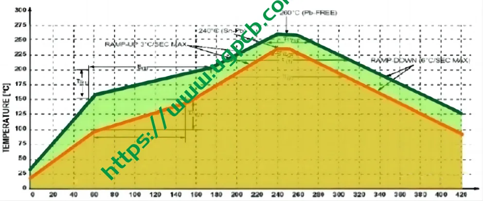
This figure compares the profiles of lead reflow and lead-free reflow. The green line covers a larger area (heat), which is the current SAC305 curve. The smaller area (heat) is the previous lead reflow. Under the premise of avoiding the explosion of the board caused by excessive high temperature and strong heat, the peak temperature of the lead-free reflow profile should not exceed 250℃. In order to maintain the same heat without damaging the PCB and components, the time of the lower peak temperature can be extended, that is, the flat-top peak temperature (240-245℃) can be extended to 10-25 seconds (depending on the size of the board). This kind of choice of lower temperature and safe heat to avoid the dangerous heat of peak temperature is what a wise person should do. This kind of risk avoidance will be very important for lead-free soldering.
In fact, from the reflow profile shown in Figure 1 above, we can see that the time that lead-free SMT soldering is above the melting point (about 217℃ for SAC305) is about 50 seconds (small board and simple parts) to 90 seconds (large board and complex parts). Such temperature and heat have certainly exceeded the Tg of various boards. For the assembled board that has been placed in such a hot environment, it has already become the α2 rubber state (Elastic Stage) with insufficient rigidity and increased weakness. Of course, it has no ability to resist any external pulling force in the Z direction.
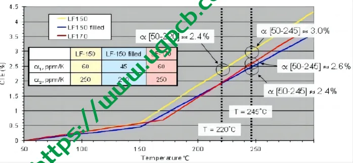
This figure was published by Mr. Wei Tianlun of Dow Chemical in the CPCA forum. The main purpose is to explain that the Z-CTE of α2 is too large, which is the main reason for the explosion of the board. The curves drawn by the three TMAs have a smaller slope on the left end, which is the α1 glass state, and the curves with a larger slope on the right end have entered the α2 rubber state. Note that the blue line of Tg150 and the red line of Tg170 have the same Z-CTE at 220℃ in lead reflow, and the risks they face are similar. Cu toate acestea, in lead-free reflow, the Z-CTE of the high Tg red line is higher than that of the lower Tg blue line, which means that the chance of the red line exploding is greater than that of the blue line. Prin urmare, it is known that high Tg boards are not necessarily resistant to strong heat.
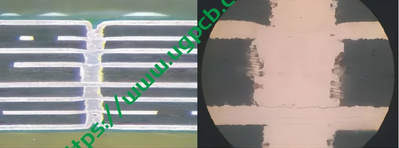
These two pictures are presented by the latest mobile phone boards, which are used to replace the ELIC stacked blind holes of PTH through holes. The left picture shows the precision stacking of 7 blind holes, so that 8 layers of copper surfaces are interconnected. The right picture shows that the detailed method starts with a double-sided board, that is, first etching a copper window on its single-sided copper foil, then burning a blind hole with a laser and filling the blind hole with electroplated copper. Then use film to press the two sides, and continue to burn blind holes and copper plating to complete multiple layers. Repeat the process to complete the layer-added mobile phone board. Cu toate acestea, although this ELIC method has many benefits, it is unavoidable that the lead-free soldering will easily explode without the help of the through-hole rivet effect.
For FR-4 board alone, its XY thermal expansion coefficient (Cte) is about 14-16ppm/℃. This excellent quality of small expansion and contraction is due to the fiberglass cloth clamping reinforcement! Cu toate acestea, the thermal expansion of the board in the Z direction has no support. Din fericire, if there are many through holes on the finished PCB, the thermal expansion rate of the hole wall copper material itself is 17ppm/℃, and the copper thickness of the good through hole (more than 1mil) and the excellent elongation (Elongation, this word is often heard by the common people as ductility) reaches 20%, which will also present a rivet-like clamping effect (Rivet Effect), which helps to suppress the Z thermal expansion of the board and reduce the risk of its bursting. As the copper plating technology for filling blind holes in current mobile phone boards (such as 3+2+3) matures, the random layer stacking blind hole method (Every Layer Interconnection; ELIC) is gradually replacing the general plated through holes. On the one hand, it can reduce costs and avoid the difficulty of filling through holes with resin, and on the other hand, it can reduce machine drilling and shorten the process. Cu toate acestea, in the absence of rivet effect, it is self-evident that it is particularly easy to explode the board.
From many latest literatures and the slices of exploded boards made by the author recently, the main reason for delamination and explosion should be: the Z-CTE of the α2 rubber state of the board is too large! IPC-4101 has adopted four new regulations as solutions for the six new “may be suitable for use in lead-free soldering” (i.e., the six new numbered boards /99, /101, /121, /124, /126 şi /129), namely: 1. Adding inorganic fillers (Fillers) to the resin 2. Specifying the minimum threshold of thermal cracking temperature Td (e.g., /99 is 325℃) 3. Specifying the upper limit of Z-CTE of α2 of the six boards to 300ppm/℃ 4. Specifying the minimum thermal cracking resistance time, such as the lower limit of TMA288 (T288) is 5 minute, etc. Cu toate acestea, even if all the six specifications of the commercial boards meet these latest requirements, it cannot guarantee that the PCB will not explode during the reflow process of downstream assembly. Of course, it also involves the influence of the PCB process itself (such as the response of the press management and PTH and copper electroplating processes), the quality and quality of the downstream reflow furnace and reflow profile (Profile), and even the difference in CTE between components and boards under strong heat. The latter causes the weak board to be torn by components, which is not yet controlled by CCL or PCB manufacturers.
2.The difference between self-explosion and external force cracking
2.1 Causes and phenomena of self-explosion
The main reason for the explosion of various multilayer boards is that the Z-CTE of the resin itself is too large in the strong heat α2 rubber state. This kind of cracking in the thickness direction will come from different failure modes such as poor affinity between glass fiber and resin, poor adhesion between resin and copper foil black film, or insufficient degree of cure of the resin itself and self-cracking. With the help of many other internal and external factors, it is almost impossible to completely avoid lead-free soldering and avoid board explosion. Examples of such additional factors are as follows:
2.1.1. Heat concentration areas where many PTHs are densely packed in multi-layer boards.
2.1. 2. Large copper surface areas without PTHs to help clamp are also prone to board explosion. Because the total Z-CTE of PCB’s Z-direction thermal expansion, including α1 and α2, is about 3.5%, and the CTE of the copper hole wall is 17ppm/℃, and when the copper thickness exceeds 1mil and the elongation can reach 20%, the PTH copper wall should have an anti-explosion rivet effect.
2.1.3. The new HDI mobile phone board of arbitrary layer interconnection (ELIC) no longer has orthodox PTH, but instead uses multiple copper-filled stacked blind holes. This multi-layer board without rivets is also prone to board explosion.
2.1.4. Multilayer boards are subject to mechanical external impact, so that the damaged areas of the structure are also prone to board explosion, such as rough V-cut or punching.
2.1.5. As for the poor quality of the downstream assembly customers’ reflow furnace, the improper measurement method and poor management of the lead-free reflow profile (Profile), etc., can also cause some board explosions. De exemplu: the heating rate (also known as the slope) at the beginning of the reflow curve is too fast, causing the PCB surface to overheat while the board has not had time to heat up. Under the shear force of uneven thermal expansion, the weaker parts of the structure are prone to blistering. The slope of this heating section (Ramp up) must be adjusted within a range of 1℃-3℃/sec according to the size of the board and the number of parts.
2.1.6. A good reflow furnace should keep the temperature difference of the PCB board within 5℃, and the temperature difference of the waiting area of the empty furnace (which can be measured by using an aluminum plate or a special temperature measuring plate with a thermometer) should not exceed 2℃. And the rectangular board should adopt the mode of horizontal walking to shorten the temperature difference between the front and back boards.In this way, the heat drop of the board surface and the explosion of the board can be reduced.
2.1. 7. For large thick boards or components with multiple BGAs, it is advisable to use a longer reflow curve with a saddle (150℃-190℃) to try to achieve uniform temperature of the entire board surface and the inside and outside of the board body (note that resin and glass fiber are both poor conductors) to reduce explosion. The slope before the peak temperature should also be controlled at about 1-3℃/sec depending on the size of the board. The peak temperature of the general assembly board should not exceed 245℃. For large boards that require more heat, the peak temperature can be extended, that is, the flat-top profile, and the peak temperature time can be extended to 20 seconds, so that the bad heat in the dangerous high temperature area (above 250℃) can be avoided.

The left picture shows the inner large copper surface area of the 12-layer board stack. The strong heat of lead-free soldering often causes multiple micro cracks between the inner layers. Usually, as long as there is no blistering or delamination of the outer layer of the multilayer board, the microcracks between the many inner layers will never be known, but the reliability (such as CAF) is inevitably full of concerns. The right picture shows a much taller 22-layer board. Because of the excellent through-hole copper wall with sufficient thickness (more than 1mil) and good elongation (mai mult decât 20%), the lack of microcracks in the board has been greatly reduced under the cooperation of the rivet effect. Cu toate acestea, once it is a thick copper multilayer board, it is another matter!

Even with the rivet effect of good quality PTH, when the Z-CTE of the board α2 is too large, after multiple reflows of bad profiles downstream, the multilayer board or thick copper multilayer board still cannot escape the fate of explosion and microcracks. For lead-free reflow of thick and multilayer large boards, the board should be high Tg (general commercial boards can be medium Tg with better toughness). PN hardening and adding filler are the right way to lead-free.

This is a long saddle profile similar to the lead reflow profile for large boards with multiple BGAs. The purpose of the long saddle is to make the board surface and the inside of the board as uniform as possible, and to allow the bottom of multiple BGAs to obtain enough heat before starting to climb to the peak temperature of strong heat, so as to reduce the board explosion and cold welding of the balls inside the BGA. Although the temperature of the lead-free reflow profile is higher, the principle of heat transfer remains unchanged.
2.2 Pad Crater of the board caused by oblique pulling
The above are all various bursting phenomena caused by the Z expansion of the board itself during strong heat. Cu toate acestea, during the assembly welding, when the thermal expansion of the components in the X, Y or Z direction is too different from that of the PCB board, the rubber-like softened board resin may also be pulled up by the components (components) together with the copper pad and the bottom substrate. This oblique pulling is completely different from the horizontal cracking of the board, and is specifically called Pad Crater. De exemplu, the lead-free solder balls with greater rigidity of BGA and the larger ceramic capacitors with greater rigidity will often pull up the copper pad and the bottom resin substrate during lead-free soldering. The lead-free solder balls with weaker rigidity and lower melting point will often be stretched and deformed to eliminate their stress when pulled in strong heat; as for the lead-free solder balls with greater rigidity (i.e., larger modulus), the copper pad and the substrate below will often be pulled up together when the BGA corner balls are not easy to stretch. In fact, if such obliquely pulled cracked substrates have not caused the wire to break, their local floating cracks will never be known and will rarely cause any disasters. Just like the various microcracks inside the multilayer board after soldering, if they have not pulled off the copper wall of the through hole, they will never be considered as any quality defects. Cu toate acestea, once the wire or hole is broken, it is bound to represent a big problem.
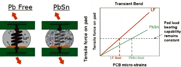
From the left diagram, we can see that the lead-free ball is very rigid, while the lead ball foot is relatively soft. Prin urmare, once subjected to external force (thermal stress or mechanical stress), the rigid solder ball will directly transfer the stress to the solder joint of the top BGA carrier board, thereby causing many internal injuries that cannot be detected by electrical testing. The right diagram shows the comparison of the Young’s Modulus (or modulus) composed of stress and strain between lead-free and lead-containing. When the lead-free ball has a larger mold (i.e., a larger slope or a larger rigidity), its strain is obviously insufficient when subjected to a certain external force impact. Cu toate acestea, the lead ball has a significantly larger strain due to its smaller slope (less rigidity and more flexibility). In other words, when subjected to external force, the lead ball that is easily deformed can absorb the impact and reduce the failure of the solder joint.
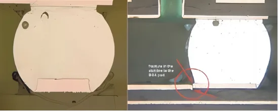
The left is the PadCrater presented in the reflow strength of the lead-free ball. Since no circuit is caused, it will never be detected by electrical testing. Cu toate acestea, when the crack has been cracked and a path has appeared, CAF will have an opportunity to harm the product. The cracks on the right have torn the wires apart, so they can’t escape the law.
BGA solder joint failure and pad cracks
Due to the strong heat of lead-free soldering, the board resin is already in a weak rubber state of α2. În plus, the CTE of the silicon chip on the top of the BGA package carrier is only 3-4Pppm/℃, and the CTE of the carrier itself XY reaches 15ppm/℃ during strong heat. The difference between the two will force the BGA carrier to warp concavely (Concave Warpage). Prin urmare, the upward pulling force on the four corners of this BGA often leads to different disasters, that is, different failure modes (Failure Mode) will be presented in vertical pulling:
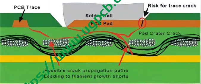
The cracks caused by vertical or oblique pulling in strong heat are mostly cracked along the interface between the glass fiber cloth and the resin or its trend. This will be related to the Silence treatment on the surface of the glass fiber cloth or the thickness of the ButterCoat. (The above three pictures and 12.13 pictures are taken from the forum held by IPC/CPCA in Shenzhen)

During the strong heat of lead-free reflow of large BGA, the substrate (substrate CTE in XY is about 14-15ppm/℃) will show a concave phenomenon due to the small CTE of the silicon chip (3-4ppm/℃). At this time, the lead solder balls on the outer line will be pulled to eliminate their stress, and the lead-free balls are more rigid and prone to the risk of breaking their heads or feet (note that this picture shows the appearance after recovery to room temperature).
3.1.If the surface film of the substrate ball bearing pad is electroplated nickel gold, it is easy to cause the solder joints on the top of the ball feet to crack and break when the gold is brittle.
3.2.Due to the oxide layer on the surface of the solder ballThicker, so that the no-clean flux of the solder paste on the PCB pad cannot be effectively removed, the solder paste cannot be completely healed with the solder ball, and the pillow effect (Head on Pillow) will easily occur. This abnormal state of seemingly close but actually separated will certainly not withstand any external force and will easily separate from the middle.
3.3. Once the ENIG surface treatment is used on the PCB ball pad due to ignorance, not only will the black pad (BlackPad) rich in phosphorus and nickel oxide occur twice in lead-free soldering, but also the AuSn4 formed by the immersion gold layer cannot be away from the interface, resulting in gold embrittlement (Gold Embrittlement), which may also cause the failure of broken pins.
3.4.For lead-free PCBs with fine pitch CSP to be soldered, when the pitch of the ball pad center approaches 0.5mm or even 0.4mm, the pad diameter of the PCB is only about 10mil or 8mil. For lead-free soldering with large surface tension, such a small pad surface should also be joined to the pad side in addition to the solderable area of the pad surface. Cu toate acestea, the ignorant upstream designers are totally unaware of lead-free and continue to use the outdated green paint on pad (SM on Pad) method, which greatly weakens the solder joint strength of the PCB ball pad. Once the PCB, especially the mobile phone board, encounters such an ignorant and ridiculous customer, the repeated claims after the broken foot due to insufficient strength are not a resentment that can be swallowed by admitting bad luck.
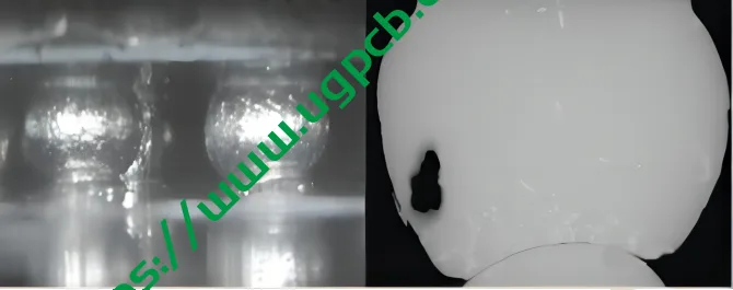
The left picture shows the appearance of the solder joint of the ball foot on the PCB after the lead-free reflow of a large BGA through an endoscope. Anyone with a discerning eye can see that the solder paste and the solder ball have not been fused to each other, which is called the pillow effect. One reason is that the reflow curve is poor and the heat of the inner ball is insufficient, which is a typical cold soldering (CodlSoldering); the second reason is that the surface of the solder ball has been severely oxidized, and the activity of the no-clean flux in the solder paste is weak, so the oxide cannot be removed and cold soldering is formed. This poor reliability will never be detected by electrical testing and is more likely to be broken by external forces.
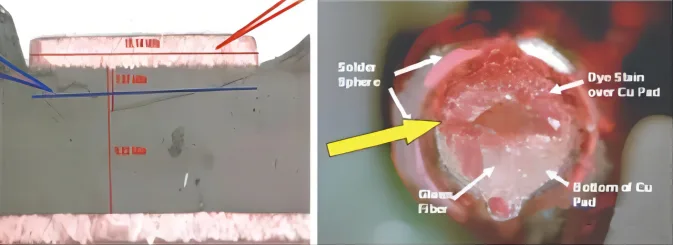
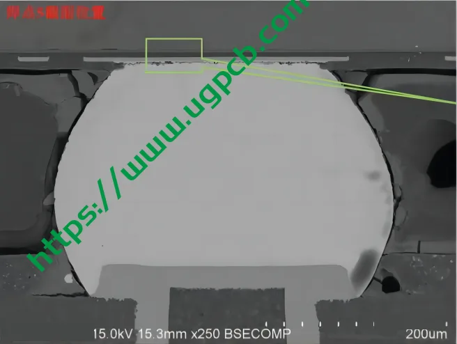
The left picture shows the pit cracking that has occurred in the strong heat, but after cooling, the substrate shrinks to its original state, but there is a crack that cannot be healed. The right picture shows the substrate attached to the copper pad after the red ink test, which is the most obvious proof of the pit cracking.
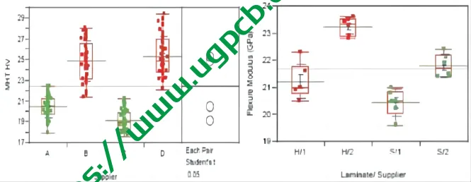
The green A and C suppliers in the left picture have a lower microhardness of the board resin, so there is no pit cracking. The red suppliers B and D used boards with a higher microhardness resin, which had cracks. The boards from suppliers H/I and H/2 on the right had higher Tg, and cracks had occurred under high modulus rigidity. As for the boards from suppliers S/1 and S/2, which were typical FR-4 with low Tg, cracks did not occur.
3.5.Din fericire, BGA did not have the above-mentioned failures in lead-free soldering. The lead-free solder balls with more obvious rigidity and greater hardness, when the carrier is pulled upward by strong heat, will directly transmit the force to the top and bottom of the ball pins, causing the head and pins to break, and it is even possible to pull out the resin at the bottom of the PCB pad and crack it obliquely. In fact, the red ink test method (Dye and Pry) can be used afterwards to determine whether such boards have cracks.
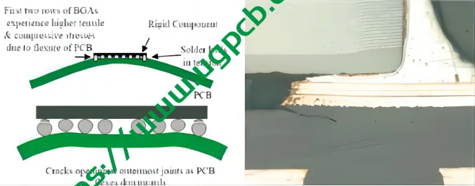
The left picture shows that the upper air temperature of lead-free reflow is 50℃ higher than the lower air temperature, which will cause the PCB to bulge and also cause the stress of BGA corners being stretched and torn. The right picture shows that when a larger capacitor is mounted on the board, its CTE is very different from the CTE of the PCB, and when the α2 board becomes soft, its pulling stress will often cause the board to be partially torn obliquely.
4.Improvement Actions
The new definition of “pad crater” was first proposed by Gary Shade of Intel Forum in March 2006. Later, Gary Long of Intel again stated it at the IPC/CPCA Forum held in Shenzhen in October 2006. The industry has organized joint research units, including well-known IT manufacturers Intel, Cisco, Jabil, Sun, IBM, Foxconn, Dell, Lenovo, Merix, Apple, Isola, Celestica, Henkel, and Dage. The work objectives of this WG will be:
4.1How to detect the pad crater that has occurred?
4.2. How to predict the pad crater that may occur?4. 3. Set the acceptance specifications for pad crater.
4.4. How to try to find the possible cause of pad crater from the quality indicators of the base board (TG, TD, PealStrength, etc.).
As for the practical improvement methods that are feasible at present, there are about:
4.1.1. Remove the three ball pins at the four corners of large BGA, or arrange non-functional fake ball pins and fake pads.
4.2.2. High-end products can fill underfill at the bottom of BGA.
4.3.3. Small BGA or CSP can apply corner glue (Cornerfill or Coner Glue) on the outer edges of the four corners.
4.4.4. For the ball pin pads at the four corners of BGA, use the method of green paint (SolderMaskDefinedLand) to strengthen the fixing force of the pads on the board surface.
4.4.5. Increase the diameter of 1 or 3 pads (even non-functional ones) at the four corners to have better grip in strong heat.
 LOGO UGPCB


