Introduction to Blind and Buried Vias PCB
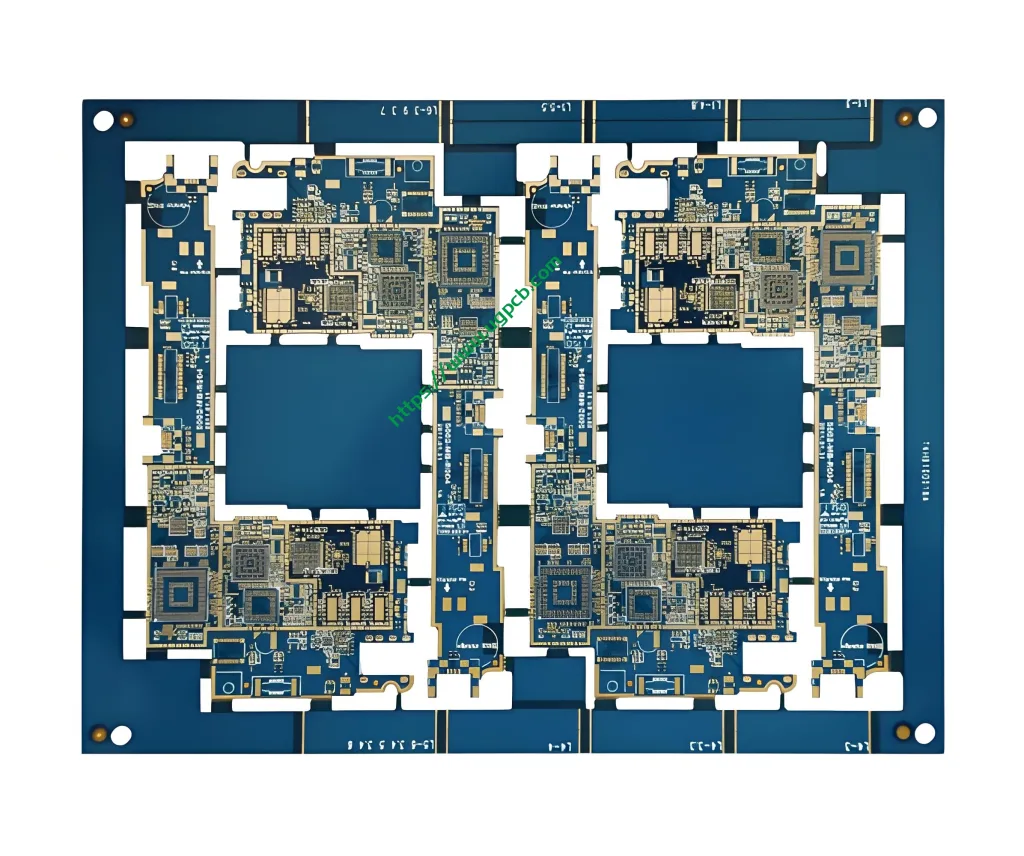
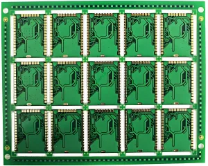
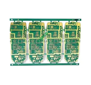
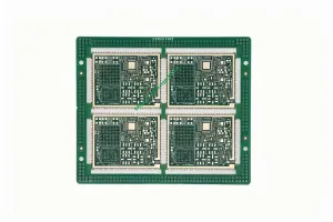
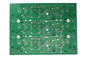
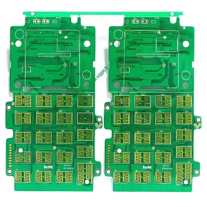
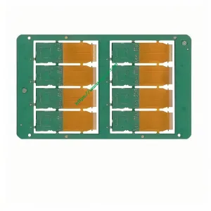
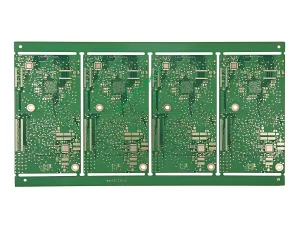
Blind and Buried Vias PCBs are advanced printed circuit boards designed for complex electronic applications. These PCBs feature blind and buried vias, which allow for intricate internal connections without compromising surface real estate. This product is ideal for high-density interconnect applications.

Purpose and Applications
Security Control PCB
Primarily used in security control systems, Blind and Buried Vias PCBs ensure reliable connectivity and data transmission in critical security setups. Their robust design makes them suitable for applications requiring high signal integrity and durability.
Classification and Materials
High TG FR4 Material
Constructed from High TG (Temperatura de tranziție a sticlei) FR4, this PCB offers excellent thermal stability and mechanical strength. The 1OZ copper thickness enhances conductivity and heat dissipation, making it suitable for high-performance applications.
Performance and Specifications
Layer Structure and Special Processes
The PCB consists of 12 layers with a unique layer structure: 1-2, 1-3, 4-6, 7-12. It incorporates blind and buried vias, which allow for complex internal connections without compromising the board’s surface real estate. The minimum hole size is 0.2mm (8mil), accommodating fine-pitch components.
Surface Treatment and Trace/Space
The surface treatment is immersion tin, providing good solderability and corrosion resistance. The trace/space configuration is 4mil/4mil (0.1MM/0.1MM), ensuring precise and dense circuitry layout.
Production Process
Steps Involved in Manufacturing
- Material Preparation: High TG FR4 boards are cut to the required dimensions.
- Layer Stacking: The layers are stacked according to the specified structure.
- Foraj: Blind and buried vias are drilled with precision.
- Plating: The holes are plated to create electrical connections between layers.
- Gravură: Unnecessary copper is removed to form the desired circuit pattern.
- Surface Treatment: The board undergoes immersion tin treatment for enhanced solderability.
- Inspecţie: Each board is thoroughly inspected to ensure quality and compliance with specifications.
Key Features and Benefits
Advanced Technology Integration
The integration of blind and buried vias allows for more complex and compact designs, reducing the overall size of the PCB while maintaining high functionality.
High Reliability and Durability
The use of High TG FR4 material ensures that the PCB can withstand high temperatures and harsh conditions, making it reliable for long-term use.
Enhanced Signal Integrity
The 1OZ copper thickness and precise trace/space configuration contribute to superior signal integrity, crucial for security control applications where data accuracy is paramount.
Use Cases and Scenarios
Security Systems
In security control systems, the Blind and Buried Vias PCB provides a stable platform for various sensors and communication devices, ensuring seamless operation and data protection.
Industrial Automation
For industrial automation, this PCB supports high-speed data transfer and robust connectivity, essential for controlling machinery and monitoring processes efficiently.
Aerospace and Defense
In aerospace and defense applications, the PCB’s high thermal stability and reliability make it suitable for mission-critical equipment and systems.
Concluzie
Blind and Buried Vias PCBs stand out as high-performance solutions for complex electronic applications, especially in security control systems. Their advanced features, robust materials, and precise manufacturing process ensure reliability and efficiency in demanding environments.
 LOGO UGPCB

