
Дизайн стека PCB
В современном электронном дизайне, печатная плата (Печатная плата) Design Stackup является одним из ключевых факторов, определяющих производительность цепи, надежность, и стоимость. Особенно когда количество слоев превышает четыре, Дизайн Stackup не только влияет на целостность сигнала, электромагнитная совместимость (ЭМС), и тепловое управление, но также напрямую влияет на производственные затраты и сложность процесса. Эта статья начнется с фундаментальных концепций, углубляться в основные принципы Печатная плата дизайн стека, выбор материала, и высокоскоростные стратегии оптимизации сигналов, Помощь инженерам принимать более обоснованные решения в процессе проектирования.
Основы дизайна стека PCB
Что такое стек PCB?
Stackup PCB относится к процессу складывания нескольких слоев ядерных впендий (Основной), препарат (Препрег, сокращено как стр), и медная фольга в определенной последовательности, которые затем ламинируют, чтобы сформировать интегрированные многослойная плата структура. Ядро дизайн Stackup заключается в рациональном распределении слоев сигналов, Силовые слои, и наземные слои, чтобы соответствовать электрическим характеристикам, механическая прочность, и требования к контролю затрат.
Для одиночного или Двойные доски, Дизайн стека относительно прост, Обычно требуется только выбор подходящей толщины платы и медной платы и веса. Однако, При разработке многослойных досок с четырьмя или более слоями, Дизайн стека становится сложным и критическим. Например, Конструкция стека 16-слойной платы должна учитывать целостность сигнала, контроль импеданса, Эмк экранирование, тепловое управление, и другие факторы.
Ключевые материалы в дизайне Stackup
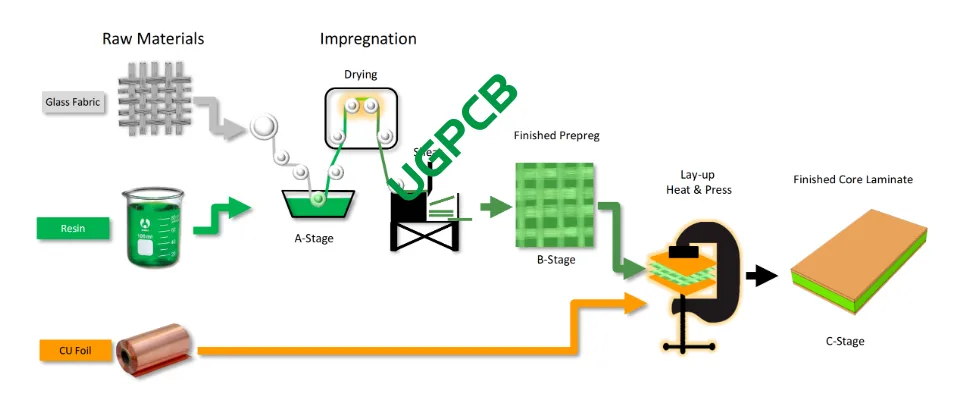
Процесс производства платы PCB Core.
- Керп с медью (Основной): Состоит из изоляционного субстрата (такие как эпоксидная смола, стекловолокно) и медная фольга, обеспечение механической поддержки и электрической изоляции.
- Препрег (Препрег): Изготовлена из стекловолоконной ткани, пропитанной эпоксидной смолой, используется для межслойной связи и изоляции.
- Медная фольга: Используется для формирования проводящих следов, с общей толщиной 0,5 унции (18мкм), 1унция (35мкм), и 2 унции (70мкм).
Основные принципы дизайна стека PCB
Распределение слоя и целостность сигнала
При разработке многослойных печатных плат, Количество слоев должно быть сначала определено на основе масштаба схемы и требований EMC. Обычно, Слои сигнала, Силовые слои, и грунтовые слои должны быть попеременно распределены, чтобы уменьшить перекрестные помехи и электромагнитные помехи. Например, Для высокоскоростных сигналов, а “GND/сигнал/GND” Рекомендуется комбинация Stackup для минимизации перекрестных соединений.
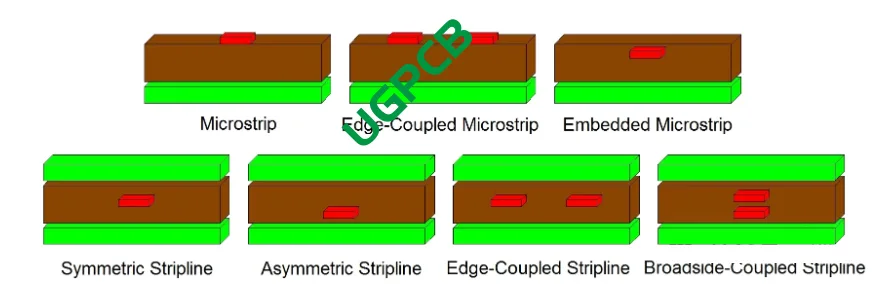
Тип микрополосковой маршрутизации
- Стрип -линия: Подходит для критических высокоскоростных сигналов, где линия сигнала зажата между двумя плоскостями заседания, обеспечение отличного экранирования.
- Микрополос: Подходит для некритических высокоскоростных сигналов, где линия сигнала находится на внешнем слое, предлагая гибкую маршрутизацию, но беднее защиту.
Контроль импеданса
Контроль импеданса является одним из основных аспектов Высокоскоростной дизайн печатной платы. Общее одностороннее импеданс-50 Ом, и дифференциальный импеданс - 100 Ом. Несоответствие импеданса может вызвать отражение сигнала, искажение, и радиация, влияет на целостность сигнала. Ключевые параметры для управления импедансом включают:
- Ширина следа и расстояние: Первичные факторы, влияющие на сопротивление.
- Диэлектрическая проницаемость: Материалы с низкой диэлектрической постоянностью помогают уменьшить задержку и потери сигнала.
- Толщина меди: Внутренние сигнальные слои обычно используют толщину меди в 0,5 унции для удовлетворения точных требований по травлению.
Управление импедансом платы PCB
EMC Design
Целью дизайна EMC является уменьшение электромагнитных помех (Эми) и улучшить возможности противоположных. Некоторые основные принципы включают:
- Смежная мощность и наземные слои: Использование межслойной емкости в качестве конденсатора сглаживания мощности при защите токов радиации.
- Маршрутизация слоев примыкает к мощности или грузовым слоям: Уменьшить помехи за счет отмены потока.
- Заземляющая плоскость как щит -слой: Подавить интерференциям RF-интерференциям общего режима и уменьшить импеданс распределения высокочастотной мощности.
Стратегии оптимизации для высокоскоростного дизайна стека PCB
Выбор материала
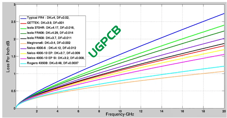
Ослабление сигналов различными типами материалов.
Высокоскоростные платы требуют материалов с низкой страной потери (Дф) и низкая диэлектрическая постоянная (Дк). Общие материалы FR-4 подходят для большинства применений, Но для высокоскоростных сценариев, Рекомендуются высокопроизводительные материалы, такие как серия Panasonic Megtron4/6. Например, Megtron6 демонстрирует потерю сигнала всего 0,85 дБ/дюйм при 28 Гбит/с, В то время как FR-4 имеет потерю до 2 дБ/дюйм.
Эффект стекловолокна и шероховатость фольги
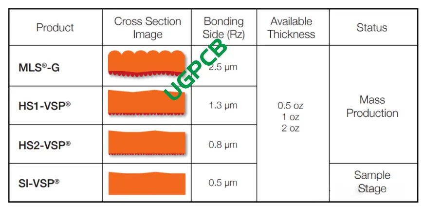
Шероховатость поверхности медной фольги с разными оценками
- Эффект стекловолокна: Стиль ткачества разных ткани из стекловолокна влияет на характеристики сигнала. Чтобы смягчить эффект стекловолокна, Выберите типы стекловолокна с минимизированными смола.
- Медная фольга шероховатость: В высокоскоростной конструкции сигнала, Шероховаство поверхности медной фольги влияет на передачу сигнала. Его влияние минимально ниже 5 ГГц, но становится значительным выше 10 ГГц.
Тепловое управление
Высокоскоростные ПХБ часто поставляются с высоким энергопотреблением, сделать тепловое управление решающим. Некоторые стратегии оптимизации включают:
- Выбор материалов высокой теплопроводности: Такие как субстраты на основе металлов (алюминий или медь).
- Проектирование тепловых прокладок и видов: Повысить эффективность теплопроводности.
- Увеличение грузовых плоскостей и областей заливания меди: Улучшить возможности рассеяния тепла.
Практические приложения дизайна стека PCB
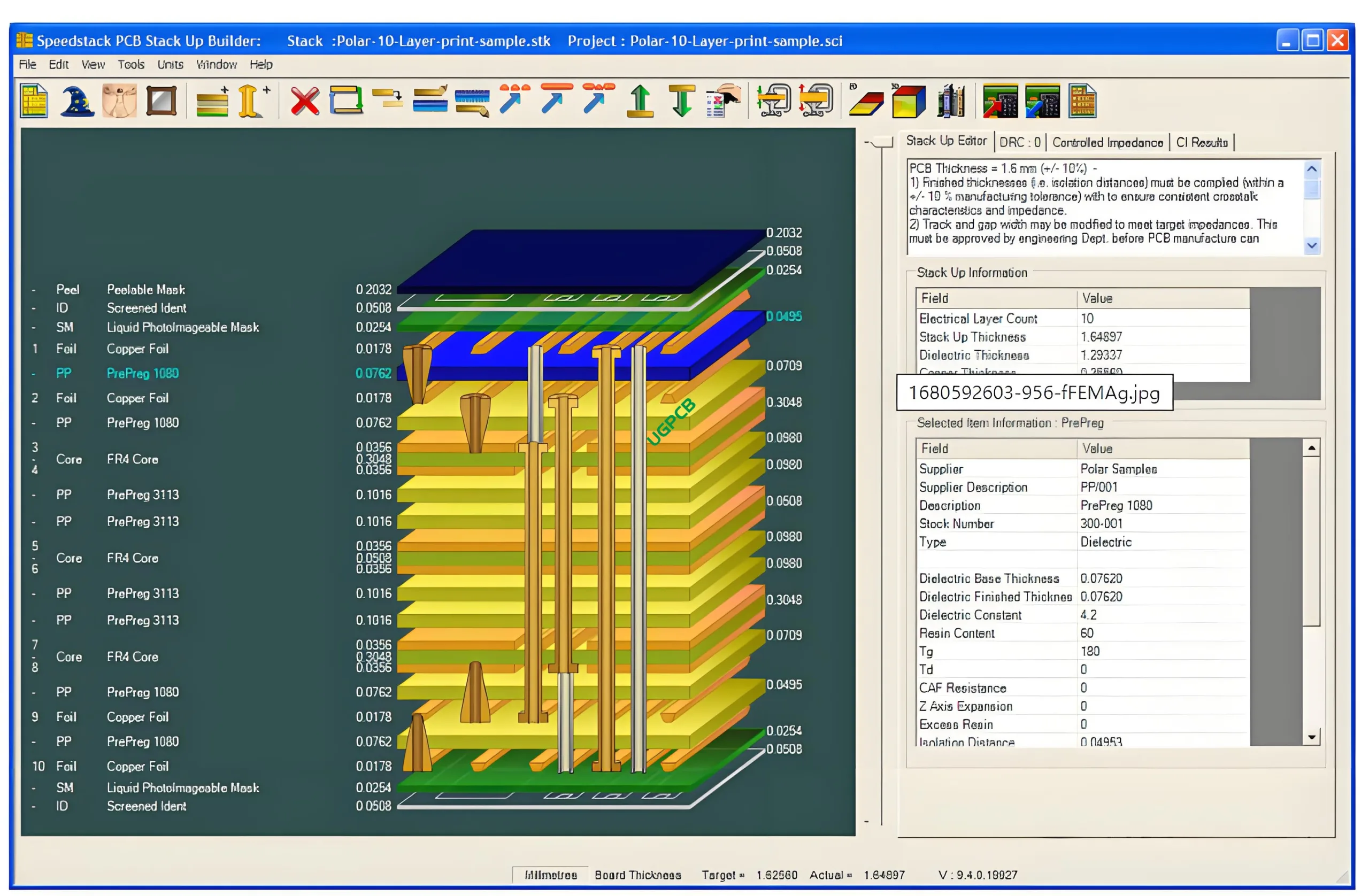
16-Слои -платы дизайн стека

16-Слои -платы дизайн стека
Взяв 16-слойную доску в качестве примера, Типичная структура стека заключается в следующем:
- Верхний слой (Сигнальный слой)
- Грунтовый слой
- Сигнальный слой
- Силовой слой
- Сигнальный слой
- Грунтовый слой
- Сигнальный слой
- Основной слой
- Сигнальный слой
- Грунтовый слой
- Сигнальный слой
- Силовой слой
- Сигнальный слой
- Грунтовый слой
- Сигнальный слой
- Нижний слой (Сигнальный слой)
Эта структура эффективно уменьшает перекрестные помехи и электромагнитные помехи, попеременно распределяя сигнальные и наземные слои при выполнении требований к контролю импеданса высокоскоростных сигналов.
Через конструкцию дизайна
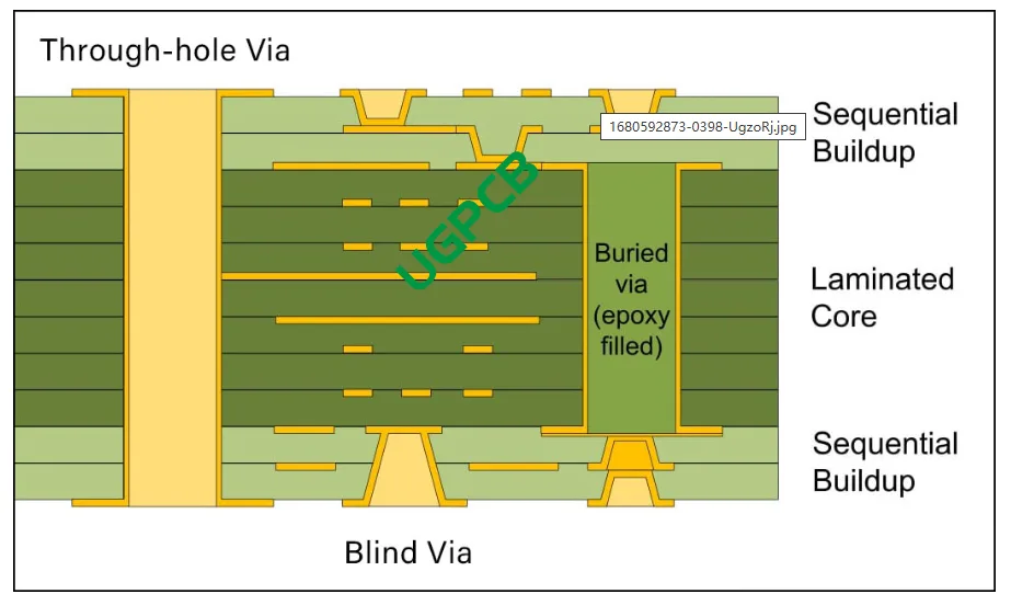
Типы отверстий платы печатной платы
В HDI PCBS, Слепые удивление и похороненные вагии широко используются для оптимизации пространства маршрутизации. Однако, Они через структуры увеличивают сложность производства и стоимость. Поэтому, через структуры должны быть упрощены во время дизайна, такие как приоритет сквозной скважины (ПТХ).
Заключение
Дизайн стека PCB - это сложная и критическая задача, включающая выбор материала, распределение слоя, контроль импеданса, EMC Design, и тепловое управление. Через рациональный дизайн стека, Производительность и надежность схемы могут быть улучшены при эффективном контроле затрат. Для высокоскоростного дизайна печатной платы, Выбор материалов с низким уровнем потери, Оптимизация эффектов из стекловолокна и шероховатости фольги, и укрепление теплового управления является ключом к обеспечению целостности сигнала и стабильности.
Являетесь ли вы новичком или опытным инженером, Освоение основных принципов и стратегий оптимизации дизайна стека PCB закладывает прочную основу для успешного проектирования электронных продуктов.
