
Введение: Industrial Significance and Technical Challenges of Via Filling
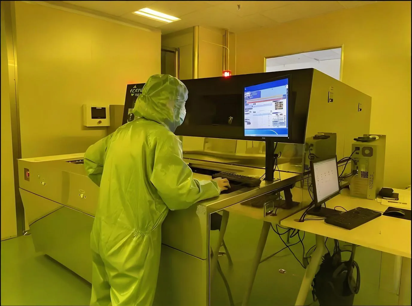
В 2023, the global печатная плата market surpassed $89.3 миллиард (Prismark), with via filling technology critically influencing over 30% yield fluctuations in 5G communication devices. This article analyzes thermodynamic equations and process matrices to reveal how via filling impacts signal integrity and thermal reliability.
1. Via Filling Technology Framework
1.1 Microvia Physics and Process Window
Per IPC-6012E, vias are defined as conductive holes ≤0.70mm (28мил). The filling process window follows:
D = (K×T)/(σ×η)
Where:
- D: Maximum fillable diameter (мм)
- Т: Substrate Tg (°С)
- σ: Resin surface tension (mN/m)
- или: Filler viscosity (Pa·s)
- К: Process coefficient (0.02–0.05)
For FR-4 substrates (Tg=140°C), filling holes >0.40mm requires материалы with σ<25mN/m and η<120Pa·s.
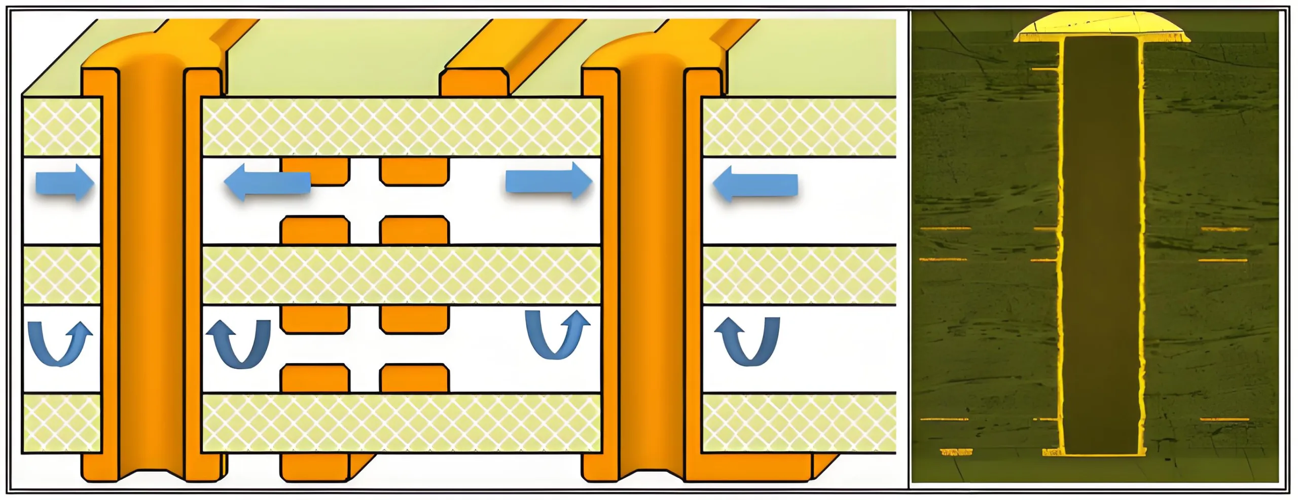
2. Resin Filling Physics
2.1 Buried Via Depth Threshold
Resin filling becomes mandatory for buried vias ≥0.8mm due to laminating flow dynamics:
P = (γ×cosθ)/(r×h)
Where:
- П: Filling pressure (МПА)
- γ: Prepreg surface tension
- θ: Contact angle
- r: Via radius
- h: Via depth
At h≥0.8mm, standard lamination pressure (3–5MPa) fails to fill voids, necessitating vacuum-assisted resin filling.

2.2 Resin vs. Lamination Filling: 6-Dimensional Comparison
| Parameter | Смола начинка | Lamination Filling |
|---|---|---|
| Thickness Uniformity | ± 5% | ±15% |
| Delamination Risk | <0.1% | 0.5–1.2% |
| Расходы | $0.35/dm² | $0.12/dm² |
| Minimum Trace Width | 50мкм | 75мкм |
| Thermal Cycles | 3,000 | 1,500 |
| Signal Loss (@10 ГГц) | 0.15dB/inch | 0.25dB/inch |
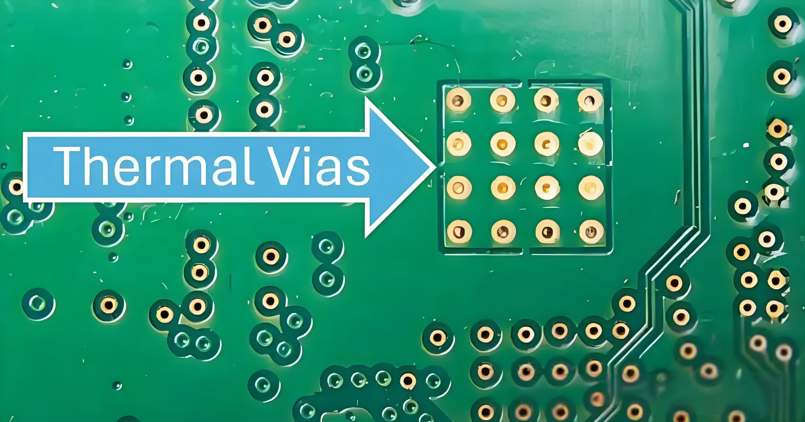
3. Solder Mask Filling Process
3.1 Ink Flow Model in Negative Imaging
Solder mask filling follows a modified Hagen-Poiseuille equation:
Q = (πr⁴ΔP)/(8μL) × (1 – e^(-t/τ))
With time constant τ=μr²/(4γ), explaining 50% fill rates in semi-filled vias when exposure time t≈τ.
3.2 HASL Board Failure Case Study
Unfilled vias in 5G base station PCBs caused tin beads, modeled by the Arrhenius equation:
t_f = A×exp(Ea/(kT))
Testing showed MTBF dropped from 10 к 2.3 years at 85°C/85%RH. Implementing 0.30mm vias with solder mask openings ≤(via diameter +0.08mm) reduced tin bead defects from 12% к 0.7%.
4. Advanced Via Filling Technologies
4.1 Conductive Filling for EMI Shielding
Silver epoxy filling enhances shielding effectiveness (SE):
SE = 20log(1/(1-ведущий)) + 10log(Н)
В 80% fill rate (ρ=0.8), SE improves by 18dB at 1GHz.
4.2 Plated Copper Filling for Signal Integrity
Copper-filled via impedance:
Z0 = (87/√ε_r)ln(5.98h/(0.8w+t))
Copper pillars reduce impedance variation from ±15% to ±5%, lowering BER from 10⁻⁶ to 10⁻¹² at 28Gbps.
5. Process Decision Framework
Total Cost of Ownership (TCO) Analysis
- Бытовая электроника: Solder mask filling offers lowest 5-year TCO
- Автомобильная промышленность: Смола + partial copper filling ensures reliability
- Military: Copper pillars optimize signal integrity
Заключение
Via Filling for 6G Applications

As terahertz frequencies demand sub-50μm via precision, nano-silver sintering emerges as a breakthrough. Mastering via filling physics will drive next-gen высокочастотная печатная плата инновации.
