
печатная плата: Фонд электронного мира
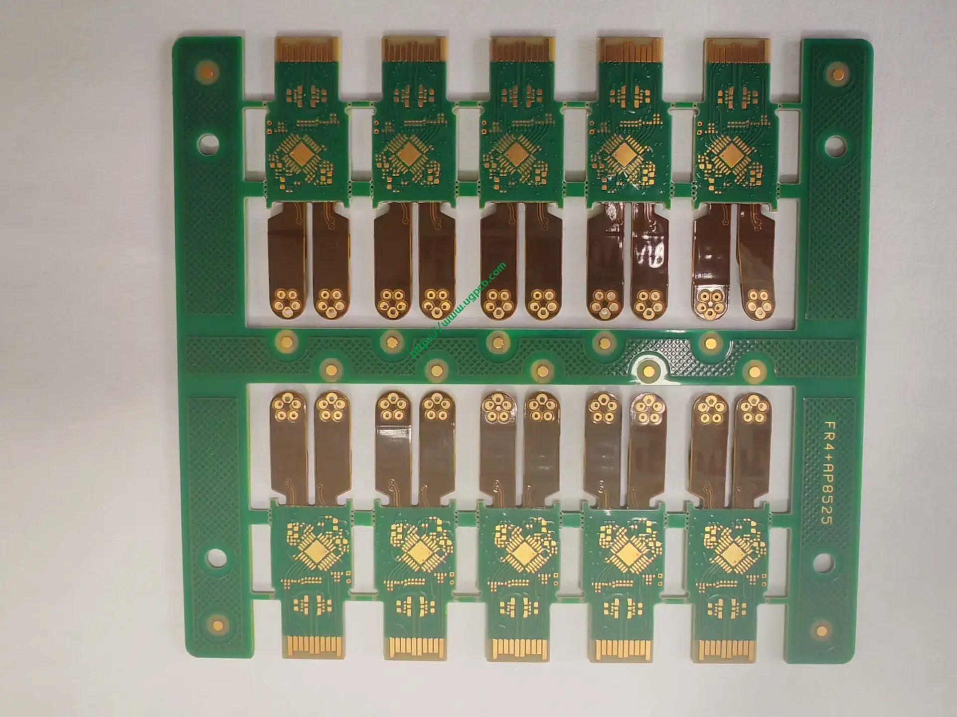
печатная плата, сокращение от печатной платы, является одним из основных компонентов электронных устройств. В качестве соединительного носителя электронных компонентов, это сделано с помощью технологии электронной печати, Отсюда и название “Печатная плата.” Субстраты печатной платы изготовлены из различных материалов, включая фенольную смолу, стекловолокно, Тефлоновый пластик, керамика, медь, и алюминий, которые выбираются на основе их изоляционных свойств и механической прочности.
печатная плата: Славное преобразование печатной платы
печатная плата, Шорт для печатной платы в сборе, готовый продукт, образованный путем сборки плат PCB с различными электронными компонентами, такими как ICS, конденсаторы, резисторы, и разъемы. На плате платы., Электронные компоненты сначала устанавливаются через SMT (Технология поверхностного крепления), а затем выводы вставляются в отверстия на доске через падение (Двойной встроенный пакет). Окончательно, После пайки и тестирования, Для пользователей создается готовый электронный продукт.
Процесс производства PCBA: От Bare Board до готового продукта
Процесс производства PCBA включает обработку SMT и обработку DIP, со следующими конкретными шагами:
-
Загрузка доски: Поместите плату PCB Bare на производственную линию для последующих операций.
-
Печать: Печать припоя пайки на пайках печатной платы для подготовки к монтажу электронных компонентов.
-
Монтаж компонента: Используйте автоматизированное оборудование или ручной труд для установки электронных компонентов на пайках печатной платы.
-
Стрелка пайки: Поместите монтированную печатную плату в пайку для переиз., где высокие температуры растопит паяную пасту, чтобы приваривать электронные компоненты на печатную плату.
-
Вставка компонентов: Для компонентов, которые необходимо установить через падение, Вставьте их булавки в отверстия на печатной плате.
-
Волновая пайка: Поместите вставленную печатную плату в волновую пайку, где расплавленная волна припоя приводит к контактам на печатную плату.
-
Тестирование и качество проверки: Провести функциональные и внешние тесты на припакованном PCBA, чтобы обеспечить качество продукта.
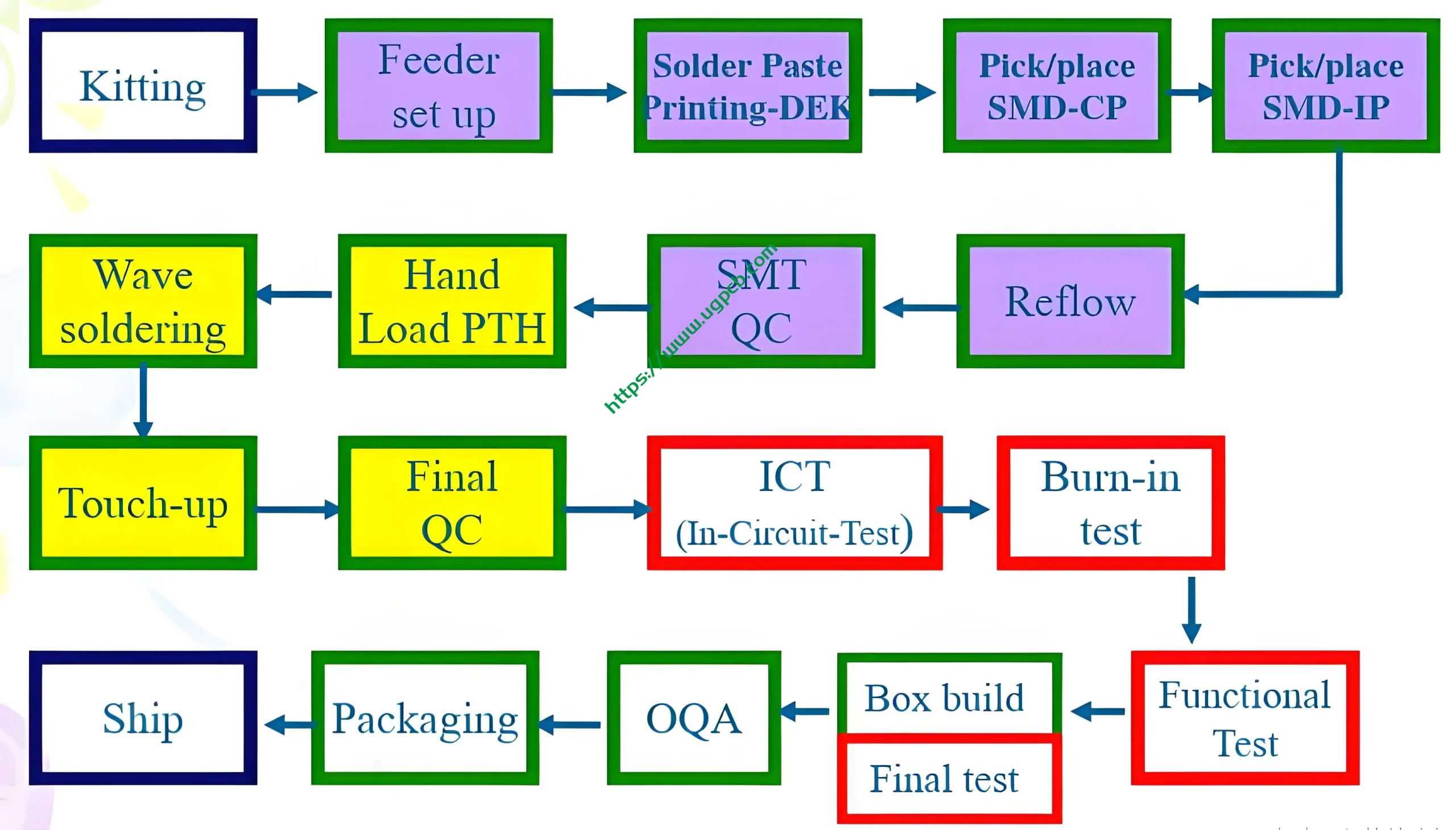
В зависимости от производственных технологий и требований, Есть различные потоки процесса PCBA, такие как односторонняя смешанная сборка, односторонняя вставка DIP, Односторонний монтаж SMT, односторонняя монтаж и двусторонняя смешанная сборка, Двусторонний монтаж SMT, и смешанные процессы вставки.
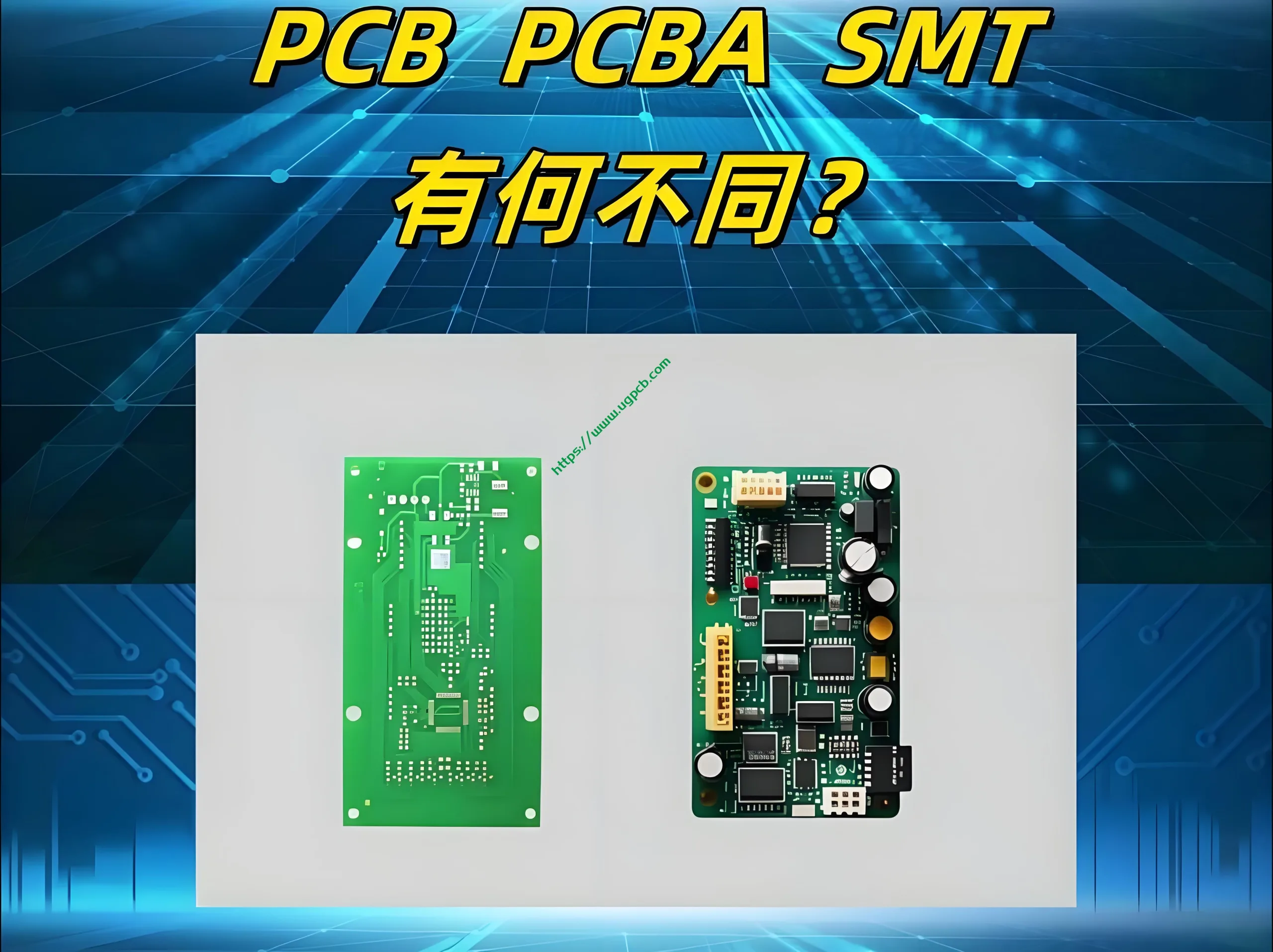
Разница между печатной платой и PCBA: От Bare Board до готового продукта
PCB - это плата без электронных компонентов, В то время как PCBA - это готовый продукт, который включает в себя электронные компоненты. Проще говоря, ПХБ - это “предшественник” PCBA, и PCBA - это “готовый продукт” сформировано после серии шагов обработки и сборки на печатной плате.
УГКПБ: Одноэтажная печатная плата,PCBA и эксперт по обслуживанию PCBA и PEVCD
UGPCB имеет многолетний опыт работы в PCBA Manufacturing и занимается предоставлением клиентам качественной универсальной печатной платы,PCBA и PEVCD Services. Мы понимаем важность каждого шага производства, Таким образом, от закупок сырья до обработки производства и качества проверки, Мы строго контролируем каждый аспект, чтобы обеспечить, чтобы каждый PCBA соответствовал требованиям и ожиданиям клиентов.
