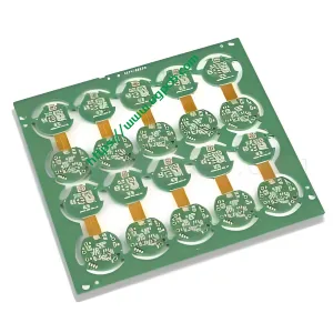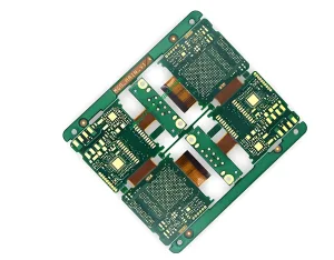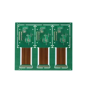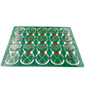
Жестко-гибкая печатная плата
Introduction to Rigid-Flex PCB
Rigid-Flex PCB combines flexible PCB (ФПК) and rigid PCB technologies. It integrates FPC’s flexibility with PCB’s structural integrity through processes like pressing, creating a hybrid circuit board tailored for complex applications.
Производственный процесс
Manufacturing Rigid-Flex PCBs requires both FPC and PCB production equipment. The workflow involves:
- Дизайн: Engineers draft circuit layouts and shapes.
- Fabrication: FPC and PCB layers are produced separately.
- Сборка: Layers are pressed together seamlessly.
- Контроль качества: Rigorous inspection precedes shipment to ensure reliability.
Definition and Core Characteristics
A Rigid-Flex PCB merges flexible and rigid circuit boards into a single structure, leveraging FPC’s bendability and PCB’s durability. This fusion enables adaptability to irregular shapes and high-stress environments.
Ключевые преимущества
-
Durability in Harsh Conditions
Resists impact and vibration, ensuring stable performance in demanding settings.
-
High-Precision Reliability
Reduces failure risks in critical systems where connectors or cables might falter.
-
Space Efficiency
Eliminates bulky connectors, optimizing component density.
-
Cost-Effective Integration
Replaces multiple rigid PCBs with a single streamlined solution.
Primary Applications
-
Industrial and Medical Equipment
Precision instruments requiring accuracy, безопасность, and soil resistance.
-
Automotive Systems
Steering wheel controls, infotainment screens, датчики, and navigation modules.
-
Бытовая электроника
Advanced features in digital cameras (DSCs) and camcorders (DVs).
-
Mobile Devices
Hinge mechanisms, camera modules, and RF components in foldable phones.
Prototype Laminate Process Considerations
- Alignment: Precision in pre-lamination processing minimizes layer misalignment.
- Material Stress: Consistent glass cloth orientation and thermal stress relief prevent warping.
- Rigid Board Thickness: Optimal thickness (0.8–1.0mm) balances stability and economy.
- Flexible Window Milling: Laser cutting ensures clean edges without compromising structural integrity.
Manufacturing Workflow
-
Выбор материала
-
Key Process Controls
- Inner layer graphic transfer
- Multi-layer flexible material alignment
- Ламинирование, бурение, and corrosion control
- Electroplating and solder mask application
-
Final Shaping
Design Guidelines
-
FPC Layer Placement
Prioritize inner layers for 8–10 layer boards (например, 4/5th layer in 8-layer stacks).
-
Bending Clearance
Maintain ≥1mm gaps between rigid and flex zones; ≥0.8mm between branch flex segments.
-
Wiring Principles
- Stagger adjacent layer traces to enhance flex life.
- Use arc transitions (≥0.5mm radius) at rigid-flex junctions.
- Avoid vias in flex zones; opt for grid copper in non-impedance-controlled signals.
-
Размещение компонентов
Keep devices ≥1mm from flex zones; use arc routing for flex-zone traces.
Rigid-Flex PCB Stackup Example
A 4-layer stackup demonstrates layer prioritization for flex integration, balancing signal integrity and mechanical stress.
Adapters and Applications
Rigid-Flex adapters facilitate testing and structural modifications in industries like automotive, медицинский, и потребительская электроника.
Cost Considerations
Higher production costs stem from material differences (thermal expansion, адгезия). Suppliers like UGPCB offer competitive pricing and end-to-end assembly services.
 ЛОГОТИП УГКПБ


Вичат
Сканируйте QR-код с помощью WeChat